Inorganic nanowire light-emitting diodes (LEDs) have held promise as inexpensive and tiny light sources, but fabrication has been challenging. Now, researchers at Cornell University (Ithaca, NY) have demonstrated a new nanofiber technology that enables on-chip light sources smaller and cheaper than LEDs, and easier to fabricate.1 The team used an electrospinning technique to form nanofibers from 150 nm to several microns in diameter and deposit them on a silicon substrate. At SPIE’s Optics + Photonics conference (Aug. 26-30; San Diego, CA), postdoctoral researcher Jason Slinker described the process and results.2
In the electrospinning process, a fluid jet lays down the delicate optical fibers, made of a solution of ruthenium tris-bipyridine dissolved in the polymer polyethylene oxide, across a spinning, gold-micropatterned silicon substrate. The jet is formed by a high voltage applied to a drop of solution on a conducting tip. The advantage of the technique is that fibers are easily deposited over gaps in the substrate, like a grid, to facilitate their mechanical, optical, and electrical properties. In this case, the nanofibers contain electroluminescent metal complexes that emit point-source illumination regularly at the gaps.
Subwavelength-size emission area
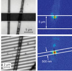
In the Cornell research, electrospun fibers measuring 1.1 µm thick emitted in very compact points along a device with a 5 µm interelectrode spacing, under an applied current of 50 V (see figure). The emission was confined to a subwavelength-size cross section measuring 240 × 325 nm2, small enough to be limited by the diffraction of an atomic-force microscope. In another trial, fibers 800 nm in diameter again showed highly localized electroluminescence on a device with 500 nm interelectrode spacing under only 4 V of current. While the emission wavelength is centered at 600 nm, the wavelength can change from blue to yellow to green by changing the fiber solution.
“What’s exciting is that these fibers offer ease of fabrication and nanoscale emission that beats the diffraction limit,” says Slinker. “Not to mention, the emission zone is smaller than what can be obtained with lenses.”
The devices with the 5 µm gaps retained 75% of their original luminescence over a 10-hour period-a relatively long lifetime, according to the researchers. Better device longevity could be obtained by encapsulating the fibers or substituting a different carrier polymer.
These micro- and nano-emitters have applications in biosensing arrays and high-resolution displays-anywhere that multiple light sources are used in parallel. A high-resolution display screen could potentially be manufactured in seconds by electrospinning red-, blue-, and green-emitting fibers across the substrate, with no additional patterning required. The nanofiber could also be coupled with a fluidic channel carrying biological molecules of interest in a lab-on-a-chip device, a small chip that performs multiple laboratory functions with minute amounts of sample fluids, making these devices “extremely attractive for medical diagnostics,” according to Slinker.
In the future, the research team, led by Cornell professors Harold Craighead, George Malliaras, and Hector Abruña, will continue work to couple these devices with fluidic channels in hopes of performing high-resolution biosensing.
REFERENCES
1. J.M. Moran-Mirabal et al., Nano Lett. 7, 458 (2007).
2. J. Slinker et al., Proc. SPIE Optics + Photonics, San Diego (2007).

