PHOTONIC FRONTIERS: PHOTONIC-CRYSTAL LASERS - Photonic crystals make nanocavity lasers

Improvements in confining excitation energy and emitted light have played a key role in the evolution of semiconductor lasers. The first diode lasers required cryogenic cooling because they were based on homojunctions. Performance improved with the introduction of single heterojunctions, then double heterojunctions, then narrow stripes, and quantum wells. Now photonic crystals are taking confinement to a new level by creating nanocavities that occupy a volume smaller than a cubic wavelength.
The goal is more than bragging rights to the world’s smallest laser. Photonic-crystal cavities control spontaneous emission, increasing the energy coupled into the laser mode and reducing laser threshold, explains Hatice Altug of the Boston University Photonics Center (Boston, MA). Because the cavity is so tiny-about a wavelength square in the device plane-direct modulation can be extremely fast. Altug and Jelena Vuckovic’s group at Stanford University (Stanford, CA) have generated 3 ps pulses by optically pumping single photonic-crystal cavities at room temperature. They project pumping with 1 ps pulses should reduce the response to 1 ps, bringing laser modulation speed to the terahertz threshold, a big allure for high-speed optical interconnects.1
Photonic crystals and nanocavities
The nanocavity in a photonic-crystal laser is a “defect” region in a microstructured region of a semiconductor. Etching an array of holes into the semiconductor creates a microstructured zone with high refractive-index contrast between the two materials-air and the high-index semiconductor. That creates a photonic bandgap, which blocks transmission of light across a wavelength range of a few hundred nanometers.
An intact region of semiconductor in the middle of the array of holes can emit light that is trapped by the surrounding microstructure (see Fig. 1). In this case, the holes are etched through multiple quantum wells in the junction layer of a III-V compound such as indium gallium arsenide phosphide (InGaAsP). The photonic crystal confines light in the junction plane of the nanocavity, so light can only escape vertically. The difference in refractive index between the semiconductor and the surrounding air provides feedback to sustain laser emission in the vertical direction.
The two-dimensional nanocavity is sized to match the wavelength of the emitted light in the semiconductor. For 1500 nm emission in InGaAsP, which has a refractive index of about 3, the cavity size is about 500 nm. This tight confinement constrains the output to a single mode perpendicular to the nanocavity. The threshold is very low, but the tiny size of the nanocavity so far has limited output of a single nanocavity to less than one microwatt.
The Q factors of photonic-crystal nanocavities are extremely high. Measured values have reached 600,000 in double-heterostructure materials, and Susumo Noda’s group at Kyoto University has written that in theory the Q might exceed 20 million if the structure was optimized.2 So far, continuous-wave operation has required cryogenic operation and optical pumping, with a 9 µW threshold demonstrated for pumping a 950 nm emitter at 780 nm. Laser threshold is higher at room temperature, at which nanocavity lasers have been limited to pulsed operation.
Higher powers can be produced by fabricating nanocavities in arrays with relatively thin photonic-crystal layers to allow coupling of electromagnetic fields between the nanocavities. For example, an array emitting at 1500 nm may have a 500 nm period, with 280-nm-thick walls. Coherent coupling of the cavities generates a single-mode beam from a small array. Output power of the array reached 12 µW, about 100 times the power from a single laser.3 The laser threshold per element in the array remains low, although the total threshold increase, and the response time slows because the array covers a larger area.
Another approach to increasing the output power of arrays is to design coupled nanocavity arrays so they emit light in the plane of the array, which allows light to be coupled from the edge of the structure into an optical fiber, considered important for some applications. Experiments at the University of Southern California, reported in May at CLEO (Baltimore, MD), transferred peak powers to 60 µW, thought to be a record, into bare multimode fibers.4
Broad-area emitters
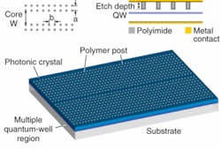
An alternative type of edge-emitting photonic-crystal laser consists of a narrow defect stripe of a row of missing holes that forms a long linear cavity. In this case, the photonic crystal consists of polymer deposited in holes etched into the semiconductor, which has a refractive index much closer to the semiconductor than air holes in nanocavity lasers. This produces effective-index guiding along the 600 µm length of the device. Although the waveguide core is only 1.5 µm wide, it produces a single transverse mode 25 µm wide, like a ridge waveguide, explains Lin Zhu, a student in Axel Scherer’s group at the California Institute of Technology (Pasadena, CA; see Fig. 2).Combining effective index guiding in the transverse direction and Bragg reflection from the photonic crystal in the longitudinal direction generates emission in both single longitudinal and transverse modes from the edge of the device. Refractive-index contrast confines light to the photonic-crystal layer. Because the structure has much larger volume than a nanocavity, the design promises higher power than nanocavities.5 The Caltech group also has demonstrated a variant that depends entirely on Bragg reflection by using angled facets to suppresses effective index guiding.6 Both are pumped electrically.
Electrical pumping
Although most nanocavity experiments still use optical pumping, many developers are pushing electrical pumping. A key problem with nanocavities has been the ability to make electrical connections.
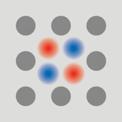
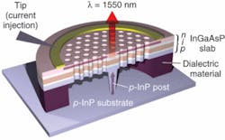
The first electronic pumping of a single-nanocavity laser was demonstrated by Yong-Hee Lee’s group at the Korea Advanced Institute of Science and Technology (Daejeon, South Korea). The group applied a ring contact to an n-type surface layer on top of a thin photonic-crystal slab, with a central post beneath the slab connecting to the p-type InP substrate (see Fig. 3).7 Recent work has improved the directionality of vertical emission from electrically excited nanocavity lasers by fabricating six photonic-crystal waveguides radiating from the cavity. “The distribution of the electrical field in the hexapole mode is very delicately balanced,” Lee reported at CLEO in May, but slightly displacing two central holes to break the symmetry can contain more than 70% of the photons within 30° of the vertical axis.8Materials and wavelengths
Much work has concentrated on the 1550 nm window of lowest optical-fiber attenuation, but that’s not entirely because of interest in communication applications. The size of nanocavities depends on the wavelength divided by the refractive index, so operating near 1550 nm allows fabrication of 500 nm cavities. Other experiments have optically excited 950 nm emission from InGaAs using GaAs pumps and cavity dimensions of 300 nm.9
Fabrication challenges increase at shorter wavelengths, but an ultraviolet photonic-crystal has been demonstrated by optically pumping a zinc oxide nanocavity with 120 nm period.10 Etching of the gallium nitride compounds used for blue and violet diode lasers remains a serious challenge.
Photonic-crystal cavities might be a key to enhancing light emission from silicon. Last year, Vuckovic’s group at Stanford showed that a single photonic-crystal cavity could enhance photoluminescence from silicon-rich film of silicon nitride by a factor of seven. The researchers reported that shortening the radiative lifetime of emitters “could be crucial for making a laser based on silicon nanocrystals,” and say that their fabrication technology is compatible with CMOS electronics.11 The researchers chose silicon nitride for the high refractive-index contrast needed for strong optical confinement.
Applications and outlook
Plenty of challenges remain for developers, particularly that of developing electrical pumping and scaling up to room-temperature operation for practical devices. Another challenge important for many applications is to develop photonic-crystal lasers that can be integrated with other optoelectronic components, and coupled to optical fibers and waveguides. Fine tuning of photonic-crystal structure will be needed to improve performance.
The range of potential applications is broad. The terahertz speeds possible with nanocavity lasers are a big advantage for optical interconnects, where limited power of single devices is not as important as it is over longer distances, says Vuckovic. Arrays could generate higher powers for moderate distances and potentially be modulated faster than current VCSELs, but electronic modulation must be developed.
Another intriguing potential use of photonic-crystal lasers is as low-jitter sources of single, indistinguishable photons, for applications in quantum information processing and related areas. Strictly speaking, such devices might not qualify as lasers if their output was spontaneously emitted photons, but in principle a photonic crystal cavity can generate nearly identical photons one at a time, and true single-photon sources have been a tough problem. Success is sure to lead to more applications.
REFERENCES
1. D. Englund et al., Appl. Physics Lett. 91, 071126 (2007).
2. B-S Song et al., Nature Materials 4, 207 (March 2005).
3. H. Altug and J. Vuckovic, IEEE Lasers and Electro-Optics Society News 20,4 (April 2006).
4. L. Lu et al., paper CMV3 at CLEO 2007.
5. L. Zhu et al., Optics Express 15, 5966 (May 14, 2007).
6. L. Zhu et al., Optics Lett. 32, 1256 (May 15, 2007).
7. H-G Park et al., Science 305, 1444 (Sept. 3, 2004).
8. H-K Park et al., paper CMV1, CLEO 2007.
9. H. Altug et al., Nature Physics 2, 484 (July 2006).
10. X. Wu et al., Appl. Physics Lett. 85, 3657, (Oct 25, 2004).
11. M. Makarova et al., Appl. Physics Lett. 89, 221101 (2006).
About the Author
Jeff Hecht
Contributing Editor
Jeff Hecht is a regular contributing editor to Laser Focus World and has been covering the laser industry for 35 years. A prolific book author, Jeff's published works include “Understanding Fiber Optics,” “Understanding Lasers,” “The Laser Guidebook,” and “Beam Weapons: The Next Arms Race.” He also has written books on the histories of lasers and fiber optics, including “City of Light: The Story of Fiber Optics,” and “Beam: The Race to Make the Laser.” Find out more at jeffhecht.com.


