NEXT-GENERATION FIBERS: Optical fibers go nano
GILBERTO BRAMBILLA
Nanoscience and nanotechnology have attracted much interest in recent years because materials exhibit novel properties when structured at nanometer dimensions. In the last two decades, nanowires and subwavelength wires have been fabricated from a variety of materials using a wide range of techniques, including electron-beam lithography, laser ablation, templates, vapor-liquid-solid techniques, physical- or chemical-vapor deposition, and sol-gel.
Although optical nanowires have previously been fabricated from silica, most have exhibited an irregular profile along their length. Surface roughness and length inhomogeneity appear to have limited the loss levels that could be reliably achieved, and thus their usefulness for optical applications.
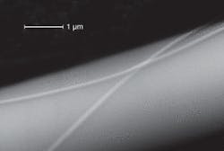
Nanowires can also be drawn from optical fibers; this process results in very low surface roughness and high homogeneity. The low optical loss of these nanowires opens the way to a host of new optical devices for communications, sensing, biology, and chemistry.
Optical-fiber nanowires are fabricated by adiabatically stretching optical fibers, preserving the original fiber dimensions at the input and output ends and allowing ready splicing to standard fibers and fiber components. These fiber pigtails have macroscopic dimensions and allow the manipulation of a single nanowire without the expensive instrumentation typical of the nano world.
Flame brushing
In the last four years, the manufacture of nanowires from optical fibers has been established as a methodology to reliably produce structures with a transmission loss low enough to be used for optical devices. Among the top-down techniques, the “flame-brushing” technique provides the longest and most uniform nanowires with the lowest measured loss. Originally developed for the manufacture of fiber tapers and couplers, flame brushing is based on a small flame moving under an optical fiber that is being stretched. The control of the flame movement and the fiber stretch can be used to define the taper shape to an extremely high degree of accuracy.
Although taper diameters in the range of 1 µm can be easily achieved with this technique, the manufacture of nanowires with 30 nm radii is an engineering challenge and requires extremely good control of the processing temperature and the airflow around the nanowire. Researchers at the University of Southampton have used the flame-brushing technique to manufacture the lowest-loss and longest nanowires to date from optical fibers. Nanowires fabricated with this technology exhibit an extremely good uniformity, with the nanowire length being millions of times larger than the diameter fluctuations. Nanowires longer than 100 mm have been manufactured and record optical losses as small as 1 dB/m measured.
Unique properties
Optical nanowires offer a number of enabling optical and mechanical properties. First, they have excellent flexibility and configurability; because of their relatively high mechanical strength, nanowires can be easily manipulated and bent. While telecom optical fibers experience considerable optical losses for bend radii smaller than 10 mm, optical nanowires can have bend radii of a few micrometers with relatively low induced loss, allowing for highly compact devices with complex geometry (see Fig. 2). Second, they have large evanescent fields; contrary to optical fibers, in which all the light is confined in the core/cladding glass structure, in optical nanowires a considerable fraction of the transmitted power can propagate in the evanescent field outside the nanowire physical boundary. And finally, they have high nonlinearity. Nonlinear processes are strongly intensity dependent, with high intensity achieved either through high-power sources or small waveguides. Compared to conventional telecom optical fibers, light in optical nanowires can be confined to an area 100 times smaller over relatively long device lengths, allowing the ready observation of nonlinear interactions such as supercontinuum generation at relatively modest power levels.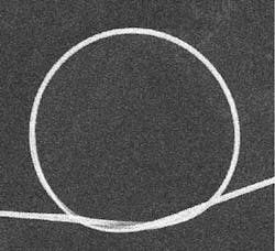
Because it exists in the surrounding medium, the evanescent field can be used as a chemical sensor. A straightforward palladium coating can result in an excellent hydrogen sensor with fast response (less than 10 s). Still, the interaction length is limited to the optical nanowire length, which is usually just a few millimeters long. By coiling the optical nanowire on itself, light is trapped in the microcoil and can make several thousand loops before reaching the output pigtail. This characteristic extends the effective length of the device, which therefore has a much longer interaction with the chemical components to sense. For example, a simple coil with a submillimeter diameter can have an interaction length greater than 1 m. Compared to other high-Q resonators, which experience considerable input/output coupling problems, the microcoil has the great advantage of an easy connection to other fiber and fiber-coupled components because it has standard fibers at the pigtailed extremities.
Chemical and biological sensing
The fiber microcoil resonator is of great interest because it has very narrow resonances—as small as a few picometers at telecom wavelengths—allowing for the manufacture of narrowband filters and high-sensitivity refractometric sensors. Refractometric sensors are chemical and biological sensors that rely on a change in the refractive index to measure the concentration of a specific chemical/biological compound. In these sensors, high Q factors (or small bandwidths) relate to a low detection limit (minimum detectable amount of analyte) and a large evanescent field to high sensitivities (shift of resonance wavelength as a consequence of a unit change in the refractive index). For this type of sensor, small size, high sensitivity, and a low detection limit are the most important criteria.
Optical nanowires are ideally suited for this application when embedded in a low-refractive-index material (see Fig. 4). Most of the area inside the resonator coils is empty, which creates an intrinsic fluidic channel to deliver samples to the sensor—unlike most ring or microsphere resonators, which require an additional channel for this purpose. A nanowire microcoil sensor can be easily manufactured by coiling the optical nanowire on a disposable rod, coating it with a low-refractive-index polymer, and removing the rod. The sensitivity of this sensor has been evaluated for different optical nanowire sizes and coating thicknesses; it has been found that for nanowire sizes of 200 nm and/or coating thicknesses of tens of nanometers, a detection limit as low as 10-7 has been achieved, meaning that it is possible to recognize a molecule of analyte in 10 million molecules of solvent. This is more than 10 times more sensitive than any sensor previously proposed.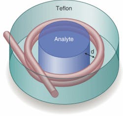
Optical manipulation
Manipulation of cells and other particles at the nanowire surface is another application for which a large evanescent field is advantageous. Light gradients have been shown to be extremely useful for trapping particles with optical tweezers. In recent years there has been increasing interest in optical manipulation at surfaces because of the possibility of continuously handling a great number of particles at the same time. This technique can be particularly advantageous in the sorting of a great number of cells in a sterile environment, as is often required in biomedical research.
Propulsion of particles along waveguides fabricated in glass or silicon nitride has been demonstrated in the last couple of years. However, because of their intrinsic nature, planar waveguides are limited to two dimensions, have a small fraction of the light propagating outside the waveguide, and present high insertion losses. In contrast, optical nanowires offer the advantage of a greater evanescent field, a 3-D flexibility, and low insertion and extraction losses (see Fig. 5).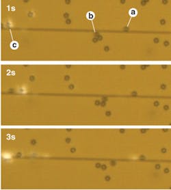
Optical propulsion can be explained in terms of the contribution of several optical forces: a gradient force drives particles up an intensity gradient and locks them to the waveguide, while absorption and scattering forces accelerate particles in the direction of the propagating field. The viscous-drag force of the surrounding medium opposes the propulsion forces and provides a limitation to continuous acceleration. The optical force experienced by the particles is proportional to the light’s optical intensity at their surface; thus, the optical nanowire’s large evanescent field and good source-to-waveguide coupling make it an excellent tool for the manipulation and sorting of particles, cells, and biomolecules.
ACKNOWLEDGMENT
The author acknowledges the financial support from EPSRC (U.K. research council) and the technical contributions from Fei Xu, Peter Horak, Senthil M. Ganapathy, James S. Wilkinson, and David J. Richardson.
Gilberto Brambilla is a Royal Society Senior Research Fellow at the Optoelectronics Research Centre, University of Southampton, Southampton SO17 1BJ, England; e-mail:[email protected].