THIN-FILM METROLOGY: Spectroscopic ellipsometer becomes industrial thin-film tool
Spectroscopic ellipsometry can precisely monitor industrial thin-film processes. In one example, it was integrated in-line to monitor thickness and quality of an oxide barrier layer deposited on a fast-moving polymer-web substrate.
ERIC TEBOUL
The last decade has seen increasing interest in the properties of thin films with nanometer-scale dimensions. Shrinking the thickness of a film to below 100 nm induces a strong correlation between the material’s optical properties and its physical dimensions. In combination with this trend, a significant portion of current research and development concerns the use of polymeric flexible materials having complex optical properties. A thin-film-metrology technique, spectroscopic ellipsometry (SE), appears to be one of the most accurate and reliable techniques for characterization of some optically transparent thin films.
Motivation for flexible substrate
Lately, research efforts have moved toward the production of flexible substrates to take advantage of the semiconducting, conducting, and light-emitting properties of organics (polymers, oligomers) and hybrids (organic-inorganic composites) through novel synthesis and self-assembly techniques. The use of flexible substrates offers significant advantages such as light weight, thinness, robustness, and the ability to be rolled. In addition, plastic-based substrates-coupled with new and smart deposition processes-open up the possibility of cost-effective and high volume roll-to-roll processing, which is attractive to packaging, optical-coating, and solar-module industries in which cost-efficient production and high-quality transparent coatings are the drivers.
For packaging applications-extensively used in food, beverage, or pharmaceutical industries-the use of flexible substrates has required the addition of a barrier layer to protect or control the contents. This material must be made as thin (for economical reasons) and optically transparent as possible. The materials used for the barrier layer are often silicon oxide, aluminum, or ceramic.
Accurate control of the film thickness is mandatory to achieve a fabrication process that gives repeatable film properties and remains cost-effective. Because of the nature of the data provided by SE, and its ability to provide them quickly, ellipsometry is a preferred nondestructive thin-film metrology technique for fast multiple film-thickness and refractive-index measurements.
Spectroscopic ellipsometry
Ellipsometry data are deduced from the more general technique called scatterometry. This optical method is currently used for critical-dimension measurements to complement information lacking from critical-dimension scanning-electron microscopy or atomic-force microscopy.
Because of its spectroscopic capability, ellipsometry is applied to a large variety of materials found in semiconductors, optical coatings, telecommunications, packaging, and nano- and biotechnology applications. Besides its high level of flexibility, SE presents certain advantages compared to other optical-thin-film metrology. Ellipsometry is nondestructive to the sample, for instance, and it has in situ and ex situ measurement capabilities and mapping capabilities. In addition to multiple film-thickness and refractive-index measurements, ellipsometric-data analysis can provide information on surface roughness, film composition, degree of crystallinity, degree of depolarization, and other film characteristics. Finally, the measurements are simple and can be made in seconds.
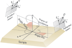
Ellipsometry is based on measurements of the changes in light polarization upon reflection from a sample surface. Unfortunately, these changes are not visible to the human eye. If we could see linearly polarized light reflecting from a flat surface, it would likely appear elliptically polarized after reflection. Indeed, the two components of the electromagnetic field-in the plane of incidence (p or TM), and perpendicular (s or TE) to the plane of incidence-experience different attenuation and phase shifts at the reflection (see Fig. 1). Ellipsometry measures the ratio of these reflection coefficients, and is usually described by a set of two data, psi and delta, related by the following expression:
null
where rp and rsare the complex reflection coefficients for TM and TE waves respectively. Because rp and rs are linked to the material refractive index through Fresnel’s law, the material’s optical properties can be derived as a function of the recorded wavelengths.
The increased sensitivity of SE stems from the fact that the polarization-altering properties of the reflecting boundary are modified significantly even when ultrathin films are present. A subangstrom change in thickness can be easily detected by a spectroscopic ellipsometer.
Experimental setup
The UVISEL, a phase-modulated spectroscopic ellipsometer (PMSE) developed at Horiba Jobin Yvon, was integrated on a reel-to-reel coater to accurately monitor thickness and quality of an oxide-barrier layer deposited on a polyethylene terephthalate (PET) substrate moving as fast as 10 m/s (see Fig. 2).
Combined with a multiwavelength detection system, the UVISEL is capable of acquiring 16 different and well-specified wavelengths in 20 ms (a multiple of 16 wavelengths can be acquired with longer acquisition time). This enabled data collection at intervals of a few centimeters along the web length; the data were fed back for immediate process adjustment. The data were acquired at an angle of 70° over the spectral range of 190 to 830 nm. In this configuration, the PMSE used two photomultiplier detectors; one for the UV-to-visible range (310-830 nm) and one for the far-UV-to-UV range (190-310 nm). The light source is a 150 W xenon lamp with high intensity in the far-UV. The full spectrum was acquired using a specially designed monochromator. All optical and polarized components of the UVISEL are suitable for the far-UV.
For two reasons a phase-modulated spectroscopic ellipsometer was chosen to monitor film thickness of the barrier layer. First, the instrument measures ∆ and Ψ throughout their full range so that thickness, optical constants, and transparency of the substrate can be characterized accurately. Second, the fast acquisition time allowed data collection at intervals of approximately 1 in. along the film length.
Measuring a barrier layer on PET
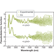
To characterize the PET and barrier layer, the optical properties of the PET substrate must be measured first to be included in the model used to calculate the thickness of the barrier layer. The PET pseudo-dielectric function was acquired by SE; between 300 and 830 nm, two distinctive types of interferences fringes related to the transparent properties of the PET were noticed (see Fig. 3). The low frequency of the oscillations is due to a crystalline-like (c-PET) overlayer, whereas the high-frequency content contains information on the total thickness of an amorphous material (a-PET). To fit the experimental data, a four-layer model (air/c-PET/a-PET/air) was used in combination with the Tauc-Lorentz oscillator model for the description of the dispersion relations. Thicknesses of approximately 500 and 1000 nm were found for c‑PET and a‑PET, respectively.
A one-layer model was used to accurately describe the barrier coating. A classical Lorentz-oscillator formula was adopted to compute thickness, refractive index, and extinction coefficient of the barrier layer. As expected, the barrier layer acts like a transparent oxide with a monotonic decrease of the refractive index and an extinction coefficient equal to zero.
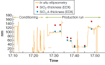
Once the optical properties of the PET substrate and top layer have been measured, they are used as starting parameters for the real-time thickness monitoring of the barrier layer. For the first 17 minutes of the deposition process, a conditioning step was performed to optimize the deposition parameters. During the deposition step, the ellipsometer acquired data every 20 ms to detect quick changes in thickness. The SE technique was used to measure the thickness of the barrier layer during the deposition process (see Fig.4). The film thickness was varied between 30 and 120 nm; even though these variations along the film length are significant, the selected ellipsometric model remains robust and gives accurate results.
On the same sample and at the same locations, the thickness measured by SE was compared to the thickness measured by another technique, electron-dispersive x-ray spectroscopy (EDX). Both techniques show the same relative trends, accentuating the reliability of the results obtained by SE.
Nondestructive, fast, and easy to use, SE is an excellent candidate for thin-film metrology. When compared to other polarization techniques, the use of phase modulation allows rapid monitoring of transparent thin-film thickness on flexible (and transparent) substrates. In the packaging industry, as well as in some microelectronics applications such as encapsulation of photovoltaic cells and organic LEDs, thickness control is required to reduce costs of materials and energy consumption. Spectroscopic ellipsometry is suitable for real-time film thickness monitoring and will serve to meet these goals.
ERIC TEBOUL is director of the thin-film division of Horiba Jobin Yvon, 3880 Park Avenue, Edison, NJ 08820; e-mail: [email protected].


