PHOTOVOLTAICS: Research targets more-efficient photovoltaics

Photovoltaic cells have existed since the late 19th century, but they still generate only a minuscule amount of energy around the world because—with a few exceptions—it is far more expensive to generate electricity with photovoltaic (PV) cells than with fossil fuels. If a connection to the electric grid is handy (as it is for most of North America), buying electricity from a utility is almost always cheaper than generating solar energy. Generating costs for PV systems average $0.30 to $0.40 per kilowatt hour, while most grid-connected U.S. electricity consumers pay only about $0.10 per kilowatt hour.
The market for photovoltaics, although very small in the overall scheme of energy generators, has been growing at 25% to 30% per year for the last several years. One effect of this growth has been a shortage in the highly purified polycrystalline silicon used to make most commercial cells, although there may be workarounds that allow the use of less-pure silicon (see “Engineering around impurities”). The shortage is expected to ease by 2008, but even with the higher prices caused by the shortage, demand is high.
One reason the technology is costly is that today’s commercial solar cells are inefficient. Most of the photons are thrown away when harvesting the energy in sunlight. Many photons don’t get absorbed at all in the semiconductor. Photons with energy below the material’s bandgap (that is, with wavelengths too long) don’t generate electron-hole pairs (see Fig. 1). Photons with energies above the bandgap deposit too much energy into the material, which can make electron-hole pairs, but also create heat, which tends to reduce efficiency. Additional losses arise from electrons and holes recombining in the cell.
In silicon, the theoretical upper limit for light-to-electricity efficiency, under normal full-sun illumination, is only 31%. This limit is largely a result of silicon’s 1.1 eV bandgap, corresponding to a photon with wavelength of 1127 nm. In practice, systems using crystalline silicon PV are about 15% efficient. To date, the most efficient PV cell is a three-junction indium gallium phosphide/indium gallium arsenide/germanium cell, which boosts the light-to-electricity conversion efficiency to 37%. Fundamentally different devices, however, could have theoretical efficiencies as high as 87%.
Radical change
If PV cells are ever to be commercially competitive with fossil fuels (assuming they stay at roughly the same price), radically different technical approaches may be required. Martin Green of the University of New South Wales (Sydney, Australia) believes that prices for low-defect, high-efficiency single-crystal PV cells are unlikely to be driven lower than US$1 per watt.1 Growth techniques that are less expensive than growing crystalline cells and that use less energy, like vapor deposition and electroplating, can bring costs down but also result in lower-efficiency devices. For solar cells to really be cost-efficient, Green argues, we need to find ways to exceed that 31% theoretical solar conversion-efficiency limit for a single-energy-threshold material. A number of research groups are working to achieve this limit by developing cells with multiple energy thresholds, or changing the incoming light to a useful wavelength, or using the extra heat deposited in the cell to improve efficiency. A multimillion-dollar program funded by DARPA (Defense Advanced Research Projects Agency) to create high-efficiency cells will probably use several of these approaches.
One promising method to increase efficiency is to engineer the bandgap using quantum wells or quantum dots so that the cell produces electrons from photons at many wavelengths. Two sessions at the 2006 Materials Research Society Spring Meeting (April 17-21; San Francisco, CA) focused on work in this field.
Organics
Despite the emphasis on raising efficiencies, the most cost-effective route to wide use of photovoltaics may be to create lower-efficiency cells very cheaply. Thin-film and organic photovoltaics can be made using low-cost fabrication methods such as solution processing, printing, and possibly even molecular self-assembly.2
Last year at the University of California-Berkeley and Lawrence Livermore National Lab (Livermore, CA), Ilan Gur and others used organic-processing methods to create inorganic thin-film PV cells.3 They made an ultrathin single-junction cadmium selenide (CdSe)/cadmium telluride (CdTe) inorganic solar cell using a typical organic processing method. They mixed roughly 30 nm long rod-shaped nanocrystals of each material in separate colloidal suspensions. Then the researchers spin-cast CdTe onto a metallized substrate. After annealing the CdTe, the suspension containing the CdSe was also spin-cast. The resulting prototype device had an efficiency of 3%—matching typical devices based on organic polymers.
The efficiencies of organics are increasing. In 2005, three research groups each reported organic photovoltaic cells with efficiencies greater than 5%. David Carroll’s group at Wake Forest University (Winston-Salem, NC), Alan Heeger’s group at University of California at Santa Barbara, and Yang Yang’s group at the University of California-Los Angeles, all published work in which the structure of the cell was carefully controlled to increase the efficiency.4, 5, 6 Although this is lower than the efficiency of a conventional crystalline silicon cell, it’s a big step forward for a technology previously stymied at around 3% efficiency.
For David Carroll’s group, the increase was made possible by creating a structure on the micron scale from a mixture of a polymer and nanostructures (fullerenes), combined with the use of a novel annealing technique (see Fig. 2). The Wake Forest researchers had known that dispersing a molecule incorporating a C61 fullerene into the light-absorbing semiconducting polymer creates acceptor sites for photon-generated electrons, thus reducing recombination rates and boosting efficiency. By heating and cooling this mixture they were able to create a more regular internal structure, further lower recombination rates, and double previous efficiency levels for this type of cell.
REFERENCES
1. M.A. Green, “Third Generation Photovoltaics: Advanced Solar Energy Conversion,” Springer Series in Photonics (2003).
2. L. Gasman, NanoMarkets (March 2006).
3. I. Gur et al., Science 310 (5747) 462 (Oct. 21, 2005).
4. M. Reyes-Reyes et al., Org. Lett. 7 (26) 5749 (2005).
5. W. Ma et al., Advanced Functional Materials 15 (10), 1617 (2005).
6. Y. Shao and Y. Yang, Advanced Materials 17 (23), 2841 (2005).
Engineering around impurities
The market for photovoltaics has been growing faster than the available supply of polysilicon feedstock. The same material is also the feedstock for making integrated circuits. The world annual production is about 30,000 tons, and although the PV community has been growing, the feedstock production has not (yet) increased. In 2004, the demand for silicon feedstock exceeded supply, and the shortage is expected to last until about 2008.
In the early years of this decade, silicon was cheap; now, the prices have doubled. Unlike the microelectronics market, the solar market requires sheer acreage for the final product, and the problem is acute: the price of silicon is roughly half the price of the final cell. One proposal for dealing with the shortage of electronics-grade silicon is to use silicon with more impurities. A “solar grade” of silicon has been proposed over the past several years. One problem with this proposal is that the less-refined silicon contains metal impurities, which reduce carrier diffusion lengths—one of the parameters that would ideally be maximized in a solar cell (see figure).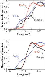
Tonio Buonassisi at the University of California at Berkeley and others recently proposed a method of managing, rather than eliminating, these impurities.1 The group studied intentionally contaminated materials and found that the spatial distribution, as well as the overall concentration of metals, determines how much damage the metals do to the cell’s efficiency.
They found that by heating and then slowly cooling (at a rate of 3ºC to 8ºC per second) the samples, the predominant type of defect changed to one in which most of the metal clumps into micron-size inclusions that have little effect on the minority carrier diffusion length. Buonassi and colleagues have not yet reported testing this on solar cells. They suggest that in addition to annealing methods, it might be possible to engineer the defects during crystal growth.
REFERENCE
1. T. Buonassisi et al., “Engineering metal-impurity nanodefects for low-cost solar cells” Nature Materials 4, September 2005.