Diamond heat spreaders maximize emitter power and lifetime
The heat-spreader assembly can be a major bottleneck for thermal management of junction temperature of optoelectronic and electronic devices. With high thermal conductivity, diamond heat spreaders can improve the cooling capability of a chip.
JERRY ZIMMER AND EDWARD PALEN
The ability to increase the optical output power of laser diodes and light-emitting diodes (LEDs) without reducing device reliability or lifetime is highly constrained by device packaging methods and materials choices. Thermal management of the laser and LED junction temperature is dominated by the heat spreader attached to the chip as part of the total assembly.
Heat-spreader function
Heat spreaders rapidly remove heat generated by optoelectronic device emitters through thermal conduction to a heat sink. The heat spreader also spreads the heat from the smaller area of the chip to the larger heat sink. Optoelectronic device performance, such as emitted-light wavelength and conversion efficiency, is dependent upon the junction temperature on the chip-lower junction temperature means better device performance and longer lifetime.
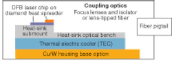
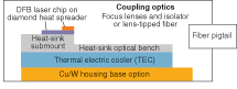
In a distributed-feedback (DFB) edge-emitting laser, the laser chip sits on its heat spreader, which then rests on top of a heat-sink submount and optical bench (see Fig. 1). Underneath the optical bench, a thermoelectric cooler (TEC) can be placed for active temperature control. The heat-sink optical bench or TEC is attached to the device package base through which laser chip and TEC heat is discharged to the printed-circuit-board (PCB) mount. Common device configurations include butterfly, dual-inline (DIL) and mini-DIL Kovar packages, TO-can packages, as well as other small-form-factor (SFF) configurations.
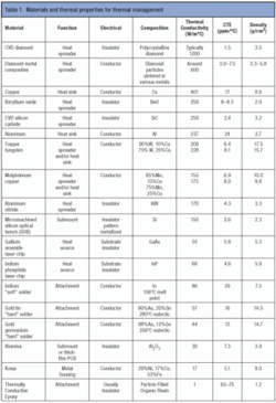
Assembly of these lasers involves multiple subcomponent attachment process steps, typically using a variety of hard and soft solders. Attachment of the laser chip to the heat spreader is at the top of this solder hierarchy with gold tin (AuSn) or gold germanium (AuGe) hard solders. Devices with fewer assembly attachment steps may use lower-temperature solders such as indium. Common heat spreaders include diamond, aluminum nitride (AlN), and beryllium oxide (BeO). High-power laser chips and LEDs typically use copper heat sinks
Thermal management
The heat-spreader assembly is a major bottleneck for management of junction temperature. Therefore, successful device manufacturers must pay special attention to materials choice and heat-spreader assembly design.
When compared to conventional materials, chemical-vapor-deposition (CVD) diamond is emerging as an effective heat spreader by a large margin. Diamond has a much greater thermal conductivity than other material choices-three times greater than copper, five times greater than AlN or BeO, and five times greater than refractory metals such as copper tungsten or molybdenum copper (see Table 1). Diamond-metal composites made from diamond particles sintered in various metal choices can provide tailoring of heat-spreader coefficient of thermal expansion (CTE) with thermal conductivities better than copper but half that of CVD diamond.
Depending on attachment choices, use of diamond for thermal management in laser devices can improve the cooling capability of the chip in assembled devices from 30% to 100%.
Diamond-cooling results
The Kinik Company of Taiwan demonstrated the superior cooling capability of diamond heat spreaders relative to conventional ceramic heat spreaders in 2003. Computer chips were mounted on heat spreaders and operated at power levels that produced a constant 110°C chip junction temperature (see Table 2). Diamond heat spreaders of the same thickness were able to remove 7.6 times more heat than alumina heat spreaders and 4.1 times more heat than BeO heat spreaders.

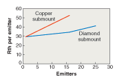
In another example of improved optoelectronic device power enabled by using diamond, the thermal resistivity (Rth) of multiple-emitter vertical-cavity surface-emitting arrays was measured on copper and diamond substrates and the Rth with the diamond substrate was 34.5% less than with the copper (see Fig. 2).
null
Package integration
While benefits in device thermal management by using diamond are apparent, implementation of diamond heat spreaders into laser and LED chips is not obvious because of mechanical stress concerns caused by the lower CTE of diamond.
Diamond is an electrical insulator. It is metallized-typically using titanium/platinum/gold (Ti/Pt/Au)-on top and bottom surfaces for solder attachment to the laser chip and for solder attachment to the heat sink on the opposite side. Prior to metallization, the top side of the heat spreader is polished smooth. This flat (less than 80 nm Ra or arithmetic average) top is used to solder-attach laser chips or LEDs, whose crystalline substrate materials-gallium arsenide (GaAs), indium phosphide (InP), or gallium nitride (GaN)-are sensitive to tensile fracture. The smooth diamond surface minimizes chip fracture issues for the assembly. The rougher (less than 5 µm Ra) bottom of the heat spreader is used to thermally attach it to the heat sink where surface finish is not an issue for solder or epoxy attachment reliability.
Because the CTE of diamond (1.5 ppm/°C) is lower than the fragile crystalline chip substrates, it shrinks less than the chip upon solidification of the attachment solder. High-temperature attachment solders of AuSn and AuGe (280°C and 356°C eutectic) have a higher Young’s modulus and a larger CTE (13 to 16 ppm/°C), than the chip CTE (5.8 ppm/°C for GaAs). The stiffness of these hard solders also helps minimize transfer of tensile load to the laser chip from the differential thermal contraction of the chip and the heat-spreader assembly.
Thermal resistance from attachment materials can contribute significantly to the total assembly thermal resistance, making it another critical factor in overall thermal device management. Attachment options include hard solders, soft solders, and thermally conductive epoxies. Lower thermal conduction resistance for assemblies is achieved by using thinner attachment layer thicknesses and by using metallic solder attachment material rather than epoxy attachment material.
High-temperature hard solders are needed for laser chip attachment to the heat spreader because this is the initial solder process in the hierarchy of solders used in the overall assembly process. Solder attachments that occur later in the assembly process require a lower solder melt temperature so that the previous solder joints do not reflow. This is particularly important in maintaining the laser chip position for coupling to optical fibers. Gold enrichment, caused by diffusion of gold from the oxidation protection layer of the chip’s and heat-spreader’s solder pads raises AuSn and AuGe solder remelt temperatures significantly, allowing the use of these same solders in subsequent steps.
Heat-spreader size and thickness can be optimized for each application using thermomechanical finite-element modeling (FEM) of the assembly. For CVD diamond, optimal thickness is 400 µm based on performance and cost. Regardless of material, the rule of thumb for sizing of heat spreaders is 2.5 times the lateral dimension for edge-mounted chips and five times the lateral device dimension for chips mounted in the center of the heat spreader such as surface-emitting lasers and LEDs. In the case of lower thermal conductivity heat spreaders such as AlN and BeO, heat-spreader thickness contributes significantly to assembly thermal resistance and is usually chosen to be between one-quarter and one-half the thickness of the chip. Heat-sink dimensions are on the order of 10 times or more the size of the chip in lateral and depth directions.
New developments
Over the past few years the cost for CVD diamond decreased significantly due to its increased use in both electronic and cutting-tool applications. There has also been increased demand for higher-brightness optoelectronic devices in multiple markets.
While the cost for CVD diamond is higher on a volume basis compared to other heat-spreader materials, its bill-of-material cost is low-typically 1% to 2% of the module bill-of-materials cost, excluding the cost of the laser chip-and its use enables increases of device optical power of up to 300% at the same device junction temperature. The use of diamond heat spreaders in multiple market applications to provide dramatic device power and reliability performance improvements will continue to reduce its portion of total device cost.
JERRY ZIMMER is cofounder and CTO of sp3 Diamond Technologies, 2220 Martin Ave., Santa Clara, CA 95050, and EDWARD PALEN is a consultant at PalenSolutions Optoelectronic Packaging Consulting, P.O. Box 3192, Redwood City, CA 94064; [email protected] and [email protected]; www.sp3inc.com and www.palensolutions.com