Thin-Film Optics: Optical-correction technique makes lambda/1000 optics a reality

JOHN W. ARKWRIGHT
With the growing interest in ultra-high-precision optics for such diverse purposes as astronomical imaging, gravity-wave observatories, subnanometer optical metrology, extreme-UV lithography, and x-ray optics, demand is increasing for optical components that have unprecedented quality at all levels, from microroughness to overall shape or “figure.” While either superlative surface-microroughness values or a highly controlled figure can be achieved independently with superpolishing or single-point surface finishing techniques respectively, it is difficult to achieve both simultaneously.
At CSIRO’s Division of Industrial Physics, we have recently developed a technique that is capable of correcting the figure of optical components to subnanometer levels without degrading the microroughness.1 The technique was initially developed to correct optical-thickness variations of large-aperture Fabry-Perot etalon filters used for solar observation, but is applicable to any transmissive or reflective optical component. For transmissive optics, it is important to deposit material that is index-matched to the substrate; for example, we use tantalum pentoxide to correct lithium niobate and silicon dioxide for silica-based optics. For reflective optics, it is not necessary to index-match the corrective layer and any mechanically suitable material can be used.
Multi-aperture mask
The correction technique uses a multi-aperture mask positioned in the plume of depositing material within a physical-vapor-deposition system (see Fig. 1). For most of our work, we have been depositing tantalum pentoxide and silicon dioxide in an ion-beam-sputtering (IBS) system, but the technique has been successful using tantalum pentoxide in an electron-beam evaporator and titanium in a filtered cathodic-arc system. The mask is positioned close to, but not touching, the optical substrate and the substrate is oscillated back and forth during deposition for reasons that will become clear later.
As with any deterministic optical correction technique the first step is to measure the profile of the optic. In the case of the Fabry Perot filters, this was achieved using a novel angle-scanning metrology rig also developed at CSIRO.2 The rig generated a 2-D profile of the thickness variation of the filter substrate with subnanometer resolution; this profile was then used in combination with the inherent variation of the deposition plume itself to generate the mask used to correct the optic.
The key to the technique is in the design of the multi-aperture mask used to selectively occlude the deposition plume. The masks consist of a large number of nominally hexagonal apertures regularly spaced across the mask surface in a checkerboard fashion. The exact design of each aperture is determined by the amount of material that needs to be deposited at the corresponding location of the optic to correct for the measured nonuniformity and by the local flux of the deposition plume at that location.
The deposition plume in the IBS system, for example, has an approximately cosinusoidal variation, with a full width at half maximum of approximately 250 mm—so if equal amounts of material are needed across the surface of the optic, an aperture at the center of the plume will have half the width of a plume 125 mm from the center. Once this inherent variation is applied to the aperture widths, an additional variation is applied to each aperture width to account for the thickness required at each location to correct the optic. This results in a mask with large apertures in regions of low deposition flux and/or requiring a relatively thick corrective layer, and small apertures in regions of high deposition flux and/or requiring a thinner corrective layer.
Achieving smooth variations
In one example, a full mask is designed to correct a 37.5 mm optic (see Fig. 2). In the hexagonal aperture structure, the apexes of apertures from one row coincide with the nominally parallel sections of the apertures from the adjacent rows. This design is critical to creating a smoothly varying deposited layer because it prevents any ridges or troughs being formed as the substrate is oscillated behind the mask during deposition. The oscillation amplitude of the substrate is also critical for creating a smoothly varying layer so that by setting the amplitude exactly equal to the pitch of the apertures along the rows, a smoothly varying deposited layer is generated that compensates for the initial variation in thickness.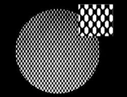
Obviously, introducing the mask between the target and substrate reduces the overall deposition rate, or utilization factor, of the system. This effect arises partly from the necessity to improve the inherent variation of the deposition plume and partly from the additional variation in aperture widths required to create the corrective layer. However, the hexagonal design of the apertures minimizes the effect because the apertures can form a close-packed pattern across the mask surface without the apertures running into each other. The maximum possible utilization factor of the mask is then determined by the amount of metal required to maintain mechanical integrity of the mask. The utilization factor of the masks depends on the thickness of the mask and the spatial resolution of the aperture pattern. In practice, utilization factors approaching 70% can be achieved for 50 µm thick masks with a 2 mm pitch between apertures on any given row.
After the mask design has been generated, it is sent to a solder stencil manufacturer for laser cutting into 50 µm thick stainless-steel sheet.3 The whole mask-fabrication process takes less than 40 minutes for a typical mask containing about 2000 apertures, so the mask can be ready for use in little more than the time taken for the return post.
Fast process
A major advantage of this technique is that the deposition process covers the whole optic at one time, so the total deposition time is much shorter than would be possible using a raster-scanned corrective technique. Typical correction times are between 300 and 700 seconds. For most purposes, a single correction is all that is required to get the error in surface figure below 1 nm root-mean-square (rms); however, for the very highest-quality optics, a second corrective layer can be deposited. For the example optic (a z-cut lithium niobate wafer), a two-stage correction process was applied (see Fig. 3). The initial thickness variation of the wafer was 11 nm rms (43 nm peak-to-peak); this was reduced to 0.41 nm rms (2.7 nm peak-to-peak) after the first run and then to 0.27 nm rms (1.9 nm peak-to-peak) after the second.
To check the effect of the correction process on the microroughness of the lithium niobate wafer, it was measured before and after correction using a Wyko topographic surface profiler with a measurement window of 117 × 154 mm2. The rms surface roughness was less than 0.2 nm (measured with a spatial resolution of 0.24 × 0.20 µm2) in both cases and was unchanged by the corrective depositions. Line scans of the thickness profile were also taken across identical sections of the wafer using the angle-scan rig before and after correction, and again, there was no change to the small-scale variation in thickness and no evidence of patterning of the surface by the discrete apertures of the mask—the thickness resolution of the angle-scan measurements was approximately 0.16 nm and the spatial resolution was about 0.5 × 0.5 mm2.
We have used this technique to correct lithium niobate wafers used for solar observation to subnanometer levels, such as the 0.27 nm rms example optic. The technique is simple to implement and can be readily retrofitted to most physical-vapor-deposition systems.
REFERENCES
1. J. Arkwright, I. Underhill, N. Pereira, and M. Gross, Optics Express 13, 2731 (2005).
2. J. Arkwright, D. Farrant, and J. Zhang, Optics Express 14, 114 (2006).
3. www.opticsinfobase.org/abstract.cfm?URI=oe-14-1-114; Mastercut Technologies, www.mastercut.com.au.
John W. Arkwright is a senior research scientist at CSIRO Industrial Physics, Bradfield Road, P. O. Box 218, Lindfield, NSW 2070, Australia; e-mail: [email protected]; www.csiro.au.