Classical models of optics essentially break down at subwavelength scales. The standard textbook view is that optical resolution is functionally limited to the order of the wavelength, both for focusing light energy onto a spot and for resolving detail in images. Yet radio-frequency devices remind us that some processes can work on submicrometer scales. Pocket-size radios have long been able to pick up 100-kHz signals in the AM frequency band, although the waves are three kilometers long.
Now optical researchers are turning their attention to subwavelength devices. The researchers have found that subwavelength resolution is possible when operating at very short distances in the near field. Subwavelength resolution is also possible with optical antennas, the nanoscale counterpart of RF antennas. Experiments have shown that thin layers of silver film with a negative refractive index can produce images with subwavelength resolution. And concepts borrowed from microwave engineering can be applied to make subwavelength optical waveguides.
Near-field optics
The nominal size of a photon is on the order of its wavelength. Light energy can be squeezed through a smaller aperture, but the transmission efficiency is low, and diffraction causes the emerging light waves to spread rapidly. This diffraction effect is also expressed as the beam divergence of a light source being proportional to the wavelength divided by the aperture. Modern subwavelength optics rely on various tricks to defeat these problem.
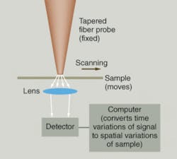
The most straightforward method is simply to make observations in the extremely near field, which is the basis of near-field scanning optical microscopy. In this case, a very thin sample is scanned within a few nanometers of the emitting aperture, so the light energy has little chance to diverge (see Fig. 1). Focusing optics collect light transmitted by the subwavelength spot that is illuminated and focus it onto a detector. These tiny-aperture probes can resolve details down to about 50 nm, but they transmit energy inefficiently and also require samples that are very thin.
Resolution can be further enhanced by tricks such as “apertureless” illumination. In this case, light from a laser beam illuminates a sharp conductive stylus that scatters the light from a subwavelength region on the tip. In this case, the optical-frequency field causes free electrons in the conductor light to oscillate at optical frequencies, producing what are called surface plasmons (see Laser Focus World, April 2005, p. 73). Surface plasmons concentrate the photon energy in a volume much smaller than a normal photon, then release the energy, effectively scattering the light from a subwavelength spot. They can achieve high intensity, making them suitable for imaging using Raman and other nonlinear processes. Although nonlinear processes are relatively weak, they occur only at points of high intensity, further increasing resolution.1, 2
Surface plasmons and optical antennas
The ability to concentrate the energy of an optical photon into a much smaller volume makes surface plasmons valuable in developing optical antennas that can transmit and receive light waves in a manner so as to effectively beat the diffraction limit. The operation of radio antennas is based on the manner in which radio waves excite motion of electrons in the conductive antenna. The excitation of surface plasmons is more complex because metals cannot be considered perfect conductors at optical frequencies, as they are at radio frequencies. But the fundamental principles are similar, and can be used to create optical nanoscale antennas that can concentrate light energy.Antenna theory is based on the interaction between an applied electromagnetic field and electrons that carry current within the conductive antenna. One example is the lightning-rod effect, which enhances electric fields near sharp points like the tip of a lightning rod. Antenna theory shows that applying an electromagnetic field enhances the electric fields at corners where the radius of curvature is much shorter than the wavelength of the applied field. This enhancement causes the antenna to emit electromagnetic waves from the zones where the field is enhanced, like the tip of the lightning rod. This effect concentrates energy to generate radiation from a spot smaller than the wavelength, as in the subwavelength tip of a conductive stylus mentioned above.
Last year a group at Stanford University (Palo Alto, CA) used this approach to design a nanoscale “bow-tie” antenna, with a pair of metal triangles arranged tip to tip, separated by a small gap (see Fig. 2, left). When illuminated by a suitable frequency, that design produces a strong electromagnetic field that is tightly concentrated near the gap between the triangles. To test the theory, the researchers photolithographically produced pairs of 75-nm gold-foil triangles with gaps of 16 to almost 500 nm, and excited them with modelocked pulses from a Ti:sapphire laser at 830 nm-a resonant frequency for the antennas with the smallest separations.3, 4 They measured the field enhancement as more than a factor of 1000 for antennas with 20-nm gaps, close to theoretical predictions. The emission was confined to a zone measuring only 650 nm2, corresponding to a spot only slightly larger than the gap.
This year the nano-optics group at the University of Basel in Switzerland made nanoscale optical antennas using the simplest type of radio antenna, the traditional resonant dipole design with two rod-shaped segments separated by a gap (see Fig. 2, right). Radio-frequency dipoles are resonant when the total length equals half the wavelength, but the lower conductivity at optical frequencies meant the resonant wavelengths were more than twice the antenna length. The group fabricated gold-film antennas 190 to 400 nm long and 45 nm wide, with 20-nm gaps in the middle, then illuminated them with femtosecond Ti:sapphire laser pulses. The researchers found the nanodipoles emitted a broad white-light continuum from 400 to beyond 800 nm, with emission strongest when the dipole was 255 nm long.5Both the Stanford and Basel experiments showed that optical antennas could absorb light energy and concentrate it into a spot only a few percent of the wavelength in diameter. That capability could find a wide range of applications from high-resolution microscopy and spectroscopy to quantum computation.
Surface plasmons also make it possible to concentrate light emitted from a subwavelength hole into a narrow beam. The trick is to surround the emitting side of the tiny hole with a periodic series of concentric metal rings (see Fig. 3). Diffracting light waves excite surface plasmons in the rings, concentrating the emerging light into a beam. A team at Louis Pasteur University (Strasbourg, France) has used this approach to create a beam diverging with full width at half maximum of ±3 degrees.6 The group suggests the technique might help reduce the divergence of emission from LEDs and diode lasers.
Negative-index lenses
Another way to achieve subwavelength resolution is with a lens having a negative refractive index. Originally proposed by theorists, negative-refractive-index materials were first demonstrated at microwave wavelengths with microstructured materials in 2001. This created a flurry of activity and led to a controversial prediction by John Pendry of Imperial College in London that a thin film with a negative refractive index could function as a “superlens,” with subwavelength resolution.7 The concept was based on collecting evanescent waves, which normally are attenuated exponentially with distance.That seemed bizarre, but this spring two separate groups described just such negative-index lenses made from silver foils only about one-eighth to one-tenth the 365-nm illumination wavelength. Silver has a negative index, but its attenuation is so high that it is considered opaque at normal thicknesses. A team at the University of California at Berkeley succeeded in imaging the word “NANO” with its negative-index lens; a team at the University of Canterbury in New Zealand imaged a diffraction grating. In both cases, resolution was about one-quarter of the illuminating wavelength.8, 9
‘Nanofibers’
Subwavelength optical fibers have also been demonstrated, based on a design for microwave dielectric waveguides. Oddly, the concept was first proposed more than 40 years ago at Standard Telecommunications Laboratories in Harlow, England, by Antoni Karbowiak, but was discarded because no one at the time could envision how to make it work. It’s now been revived as a compact waveguide for nanophotonics.
Conventional single-mode fibers are huge on a nanotechnology scale, with core diameters about five times the wavelength and 125-µm claddings. However, single-mode fiber diameter can be reduced by increasing the core-cladding refractive index. To shrink them as far as possible, Harvard University researchers drew fibers down to diameters as small as 40 nm, creating bare dielectric waveguides surrounded by air (see Fig. 4). As the diameter decreases, an increasing fraction propagates along the surface of the waveguide, as for analogous microwave guides. Attenuation for a typical 400‑nm waveguide is below 0.1 dB/mm. That is orders of magnitude higher than standard fibers, but the developers consider it promising for nanophotonics in which transmission distances would be very short.
Because light propagates on the outside of the waveguide, it can be coupled between nanofibers by touching them, without having to align their cores precisely with each other. Surface propagation makes the nanofibers potentially attractive for sensing applications. And because their diameters are so small, they can be bent very tightly.10, 11, 12
Potential applications
If the whole field of subwavelength optics leaves your head spinning, you’re not alone. Some of the seminal ideas were first shrugged off as wild theoretical speculations.
The challenge now is to find practical applications. Subwavelength imaging is not easy, but it has real attractions for high-resolution spectroscopy and microscopy. Optical antennas and negative-index lenses that can concentrate energy on subwavelength spots might help stretch semiconductor photolithography to smaller dimensions than had been thought possible. By focusing light on smaller spots, they might also expand the storage capacity of optical disks. Subwavelength fibers could enable connections between new types of nano-optical components. Although some of those applications may not happen, the most important contribution of subwavelength optics may be to build a bridge between the traditional scale of optics and the newer, smaller scale of nanotechnology.
REFERENCES
1. D. A. Higgins, Nature Materials 1, 83 (Oct 2002).
2. A. Lewis et al, Nature Biotechnology 21, 1378 (November 2003).
3. D. Fromm et al, Nano Letters 4, 957 (2004).
4. P. J. Schuck et al, Phys. Rev. Lett. 94, 107402 (Jan. 14, 2005).
5. P. Mühlschlegel et al, Science 308, 1607 (June 10, 2005).
6. H. J. Lezec et al, Science 297,820 (Aug. 2, 2002).
7. D. R. Smith et al, Science 305, 788 (Aug. 6, 2005).
8. N. Fang et al, Science 308, 534 (April 22, 2005).
9. D. O. S. Melville and R. J. Blaikie, Optics Express 13,2127 (March 21, 2005).
10. L. M. Tong et al, Nature 426, 816 (Dec. 18/25, 2003).
11. L. M. Tong et al, Optics Express 12, 1025 (2004).
12. G. Svacha et al, Paper OThA7, OFC 2005.
About the Author
Jeff Hecht
Contributing Editor
Jeff Hecht is a regular contributing editor to Laser Focus World and has been covering the laser industry for 35 years. A prolific book author, Jeff's published works include “Understanding Fiber Optics,” “Understanding Lasers,” “The Laser Guidebook,” and “Beam Weapons: The Next Arms Race.” He also has written books on the histories of lasers and fiber optics, including “City of Light: The Story of Fiber Optics,” and “Beam: The Race to Make the Laser.” Find out more at jeffhecht.com.


