Improved coatings make etalons more robust

GLEN P. CALLAHAN, EMILY KUBACKI, and LYNORE M. ABBOTT
The use of Fabry-Perot etalons has significantly improved line-narrowing of lithography sources during the past seven years. Previously, optical filters and prisms were used; however, subpicometer bandwidths and high wavefront quality can only be achieved through the use of an etalon.
Air-spaced Fabry-Perot etalons are the primary means of line-narrowing the output of both 193-nm argon fluoride (ArF) and 248-nm krypton fluoride (KrF) excimer lasers used in lithography systems. Etalons for lithography applications require high-purity excimer-grade fused-silica plates separated by a flat and parallel optically contacted glass spacer (see Fig. 1). Most etalon spacers are made from a low-thermal-expansion material such as Zerodur or ULE (ultra low expansion) glass. The inner surfaces of the fused-silica plates are coated with a reflective multilayer dielectric coating specific for the application wavelength. The outer surfaces are antireflection-coated and wedged to reduce surface losses and prevent extraneous interference patterns from forming.
An etalon is a Fabry-Perot interferometer that functions as an optical filter. It consists of two reflective plates separated by an air gap maintained by spacers. Light is reflected back and forth between the reflective plates. When twice the optical distance between the plates equals an integral number of wavelengths, the light passes through the etalon. The sharpness of the transmission peaks and the peak separation are defined as finesse and free spectral range, respectively (see Fig. 2).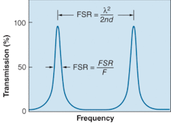
The bandwidth, or full width at half maximum (FWHM), is determined by the free spectral range (FSR) and the effective finesse (F):
FWHM = FSR/F
The thickness of the spacer (or air gap) determines the FSR, expressed in nanometers:
FSR = λ2/2nd
where λ is the wavelength, n is the refractive index, and d is the air space.
The principal factors in designing for subpicometer bandwidth are the thickness of the air gap and the effective finesse. The effective finesse is a function of reflectivity, flatness, and parallelism of the coated plates. As reflection of the coated plates approaches 100%, actual finesse is defect-limited by coating absorption and scatter, substrate surface-figure imperfections, and wedge.
Substrate-material selection, surface figure, thin-film coating materials and design, and assembly affect the bandwidth, maximum transmission, and lifetime of the etalon and subsequently the lithography system itself.
Substrate materials
Material selection, final polish, and surface quality affect performance of lithography systems and the lifetime of the optical components within them. Standard UV-grade materials have impurities that lead to low transmittance, high absorption, fluorescence, and/or color-center formation when exposed to high-photon-flux radiation. Damage-mechanism studies of standard UV-grade fused silica under long- and short-term 193- and 248-nm exposure have shown that fused silica exhibits fluorescence due to absorption by impurities. Long-term exposure also leads to eventual internal compaction within the bulk material.1, 2, 3 Internal compaction causes unwanted stress-induced birefringence in transmissive optics. Birefringence from compaction degrades the optical performance beyond the precision required in a lithography system. To avoid this, excimer-grade fused silica has been developed to minimize fluorescence and absorption in the 193- and 248-nm wavelength ranges.4
For intercavity 193- and 248-nm lenses, windows, output couplers, and end mirrors, high-purity calcium fluoride (CaF2) and magnesium fluoride (MgF2) are the preferred substrate materials because of their compatibility with the fluoride gas used in the laser resonator.
Thermal stability is critically important to maintain a constant air gap in the etalon. Etalon plates for laser line-narrowing are made from excimer-grade fused silica because it has the best thermal performance of the excimer-grade materials. The relatively large thermal-expansion coefficient prevents the use of CaF2 as etalon plates, as temperature changes impact wavelength accuracy. The thermal-expansion coefficient of CaF2 is 18.85 × 10⁻⁶/°C, versus 0.57 × 10⁻⁶/°C for excimer-grade fused silica; MgF2 is in between: 8.48 × 10⁻⁶/°C or 13.7 × 10⁻⁶/°C, depending on the crystal axis.
Air-spaced etalons can be designed as a cement-free assembly, which is especially critical for long-life performance in an ArF lithography system. Cement is particularly susceptible to degradation at 193 nm. As a result, cement-free and ring-spaced etalons have been developed by CVI. Custom ring-spaced etalons have been customer tested and survived not only long-term radiation exposure, but have also survived vibrational testing up to 28 g.
Polishing
Laser-damage thresholds and product lifetimes greatly depend on the final surface polish as determined by surface figure and surface quality.
Surface figure is a measurement of the deviation from an ideal surface in units of wavelength and in terms of peak-to-valley. Surface figure is typically measured with a test plate held in contact with the part under inspection or using a phase-shifting interferometer. A contour map of the surface is visible as light and dark bands, known as Newton’s rings or fringes. Each ring in the case of a spherical surface or line in the case of a plano surface corresponds to the deviation from ideal. The spacing between bands is equal to one-half the wavelength of the illumination source. More fringes equates to more deviation from ideal. For best image quality of the laser lithography system, surface figure should be no worse than from λ/10 to λ/20 at 633 nm after coating.
For etalons, surface figure is not enough to guarantee good performance. The single most important factor in etalon-device performance is the finesse. Since the effective finesse is a function of the flatness of each mirror and the parallelism of the spacer, etalon finesse performance is often the specified parameter. CVI’s manufacturing process for etalon plates can achieve λ/100 after coating, leading to an effective finesse of 30 or higher.
Surface quality is defined by the actual number of flaws in an optical surface in terms of scratches and digs. Scratches are defined as the apparent widths of hairline scratches allowed in the surface, specified in units of 0.001 mm. Digs are defined as the apparent diameters of defects allowed-such as pinholes, pits, bubbles, and inclusions-in a coating or surface, specified in units of 0.01-mm diameter. Most 193- and 248-nm laser optics must be specified as a 10-5 or better scratch and dig for low-scatter performance; this relates to a scratch of less than or equal to 0.01 mm and a dig of less than or equal to 0.05 mm. Surface quality is typically measured either by high-power microscopes with reticle attachments to magnify and define defect size or an optical comparator to expand the image of the optic under test. Both surface figure and surface quality specified in the preceding manner are considered laser-quality, but also are applicable to critical deep-UV (DUV) light-source-based systems in many semiconductor-processing applications.
Low-absorption, long-life coatings
Final surface cleaning of optics prior to coating is critical to ensure minimal absorption and proper performance of the coating. Good surface cleaning reduces microscopic defects in the substrate surface and coating. Microscopic defects cause increased absorption, localized heating, and ablation, leading to premature coating breakdown especially, by short wavelength laser radiation.
High-purity and low-absorbing coating materials are used to improve efficiency, laser-damage resistance, and durability of all the optics in a lithography system. Specific polarization properties can also be controlled with coating design.
For the 248-nm KrF laser line, the most common coating materials used are silicon dioxide (SiO2), aluminum oxide (Al2O3), and hafnium oxide (HfO2). For the 193-nm ArF laser line, typical materials include magnesium fluoride (MgF2), lanthanum fluoride (LaF3), yttrium fluoride (YF3), dysprosium fluoride (DyF3), thorium fluoride (ThF4), and a limited number of other fluoride and oxide dielectrics.
For most 193-nm coatings, however, the fundamental properties of the available coating materials limit the achievable reflectance and transmittance properties. In a 193-nm line-narrowed DUV beam-delivery system, some of the incident radiation can be absorbed or scattered by the beam-turning mirror coatings, so careful selection of appropriate dielectric coating materials is essential. As there are no high-index nonabsorbing materials suitable for maximum-reflectance coating designs at 193-nm, a large number of medium- and low-index coating layers are required to achieve a satisfactory mirror reflectance. Even so, a small percentage of incident laser light can be transmitted through the 193-nm mirror coating into the substrate, which makes the choice of a nonabsorbing UV-transmitting substrate such as UV-grade fused silica essential to avoid the potential of laser-induced damage at the substrate surface interface and in the bulk material.
CVI has recently improved the performance of antireflection coatings for these wavelengths for damage thresholds up to 2.5 J/cm2 at repetition rates of 20 Hz with 20-ns pulse widths. These coatings are well suited for use on transmissive and partially reflective fused-silica optics in 193- and 248‑nm laser systems. In addition, dielectric UV mirror coatings have survived low-fluence lifetime testing after six months of continuous testing. With proper care, improved coatings such as these make system downtime and frequent replacement-optic maintenance a thing of the past.
REFERENCES
1. N.F. Borrelli et al., OSA 1997.
2. N.F. Borrelli et al., 193-nm Symposium 1996.
3. P. Simon et al., OSA 1989.
4. C. Smith and B. Ackerman, Solid State Technology (2001).
Glen P. Callahan is semiconductor and technical sales manager, Emily Kubacki is a senior optical engineer, and Lynore M. Abbott is marketing communications manager at CVI Laser LLC, 200 Dorado Place SE, Albuquerque, NM 87123; e-mail: [email protected].