Nanocrystal lases in the blue at room temperature
Their size-dependent color tunability and chemical flexibility make semiconductor nanocrystals (NCs) unique as optical gain media. Although amplified spontaneous emission (ASE) and lasing at room temperature have been achieved for cadmium selenide (CdSe) NCs, ASE and lasing at blue wavelengths has never been achieved-possibly because of highly efficient nonradiative Auger relaxation processes that become dominant as the size of the NC decreases. However, by using core-shell cadmium sulfide/zinc sulfide (CdS/ZnS) NCs as an alternative gain material, researchers in the Department of Chemistry at the Massachusetts Institute of Technology (MIT; Cambridge, MA) have demonstrated both room-temperature ASE and lasing at blue wavelengths.1
Recent experiments using CdS NCs that are embedded in a host matrix result in significant deep-trap emission because of surfaces that are not well passivated. Deep-trap emission, or the emission from the recombination of trapped electrons and holes with broad energy distributions because of surface irregularities such as missing atoms, uncommon oxidation states, or adsorbed impurities, leads to a broadened emission-spectrum profile that is undesirable for optical applications that rely on the narrow emission profiles of NCs. By creating a CdS/ZnS NC-silica composite whereby CdS/ZnS core-shell NCs are chemically modified and incorporated into a sol-gel-derived silica film, the ZnS shell efficiently passivates the surface of the CdS NCs and eliminates deep-trap emission.
To create a thin film of material for ASE testing, the CdS/ZnS NCs were dispersed in ethanol, added to a silica precursor that resulted in a slightly viscous liquid that was spin-coated onto a glass slide to form a thin clear film, and then annealed. The films were then excited by the frequency-doubled output of a regeneratively amplified Ti:sapphire laser centered at 400 nm with a pulse width of 100 fs and a repetition rate of 1 kHz. The ASE spectral widths were on the order of 5 to 7 nm. After 45 minutes of continuous exposure by the high-power laser, ASE decreased in intensity to roughly half its initial value; however, the presence of ASE over such a long time period and after nearly 2.7 × 10⁶ laser shots demonstrates the good photostability of the NC-silica film.
The researchers determined that the optical gain from the CdS/ZnS NCs is due to the presence of biexcitons, as theoretically predicted. An exciton is defined as an electrically neutral excited state of an insulator or semiconductor, often regarded as a bound state of an electron and a hole. Analagous to a hydrogen molecule, excitons can bind with other excitons to form a biexciton. This finding was consistent with the observed redshift of the ASE transitions with respect to the fluorescence spectra, which can be attributed to a combination of reabsorption in the film and a negative biexciton binding energy.
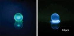
Lasing achieved
By coupling the CdS/ZnS NC-silica composite to a spherical resonator, optically pumped lasing was achieved. Nanocrystal-silica-coated spherical resonators were produced by a process similar to that for the thin films in which the NC-sol-gel mixture was spin-coated in the presence of commercially available silica microspheres onto a substrate. Under white and UV light, the microspheres fluoresce (see figure). A home-built imaging/dispersive far-field-fluorescence microscope coupled to the frequency-doubled output of the Ti:sapphire regenerative amplifier was used to excite and detect lasing from the microsphere-NC composites. By exciting individual microspheres above threshold, lasing was obtained at room temperature. A resolution-limited Q factor of greater than 600 was obtained from the spectra.
Fabricating these lasing microspheres does not require expensive lithography. The researchers are able to produce hundreds of uniform resonators on top of a single substrate, usually an inexpensive glass cover slip. “Single-mode lasing can be achieved by simply varying the size of the sphere template in accordance with the NC emission wavelength,” says researcher Preston Snee.
We have recently shown that a relatively inexpensive nanosecond pump, a Q-switched Nd:YAG laser, can also be used as an excitation source to achieve optical gain in these materials. We are currently developing the technology to electrically pump these devices.
REFERENCE:
1. Yinthai Chan et al., Appl. Phys. Lett. 86(7) 073102 (Feb. 14, 2005).
About the Author

Gail Overton
Senior Editor (2004-2020)
Gail has more than 30 years of engineering, marketing, product management, and editorial experience in the photonics and optical communications industry. Before joining the staff at Laser Focus World in 2004, she held many product management and product marketing roles in the fiber-optics industry, most notably at Hughes (El Segundo, CA), GTE Labs (Waltham, MA), Corning (Corning, NY), Photon Kinetics (Beaverton, OR), and Newport Corporation (Irvine, CA). During her marketing career, Gail published articles in WDM Solutions and Sensors magazine and traveled internationally to conduct product and sales training. Gail received her BS degree in physics, with an emphasis in optics, from San Diego State University in San Diego, CA in May 1986.