Integrated optoelectronics that leverage microelectronics technology are being developed around the world. Recent work on devices made using silicon (Si), germanium (Ge), carbon, and tin was presented in late September at the Second International Conference on Group IV Photonics (Antwerp, Belgium), sponsored by LEOS (the Laser and Electro-Optics Society; Piscataway, NJ). “The major issue for everyone is producing low-cost systems, which should open new markets,” conference chair Douglas Paul of Cambridge University (Cambridge, England) noted.
“DARPA is funding a number of programs in the U.S. attempting to make Si photonics a reality with cheap optical transceivers for Ethernet networks and ultimately chip-to-chip communications,” Paul explained. These include funding for sources, modulators, waveguides, detectors, and integration.
DARPA’s Electronic and Photonic Integrated Circuits on Silicon (EPIC) program is funding development of fully integrated Si-based nanophotonic devices through 2008, said program manager Jagdeep Shah.
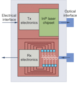
The Microphotonics Center at the Massachusetts Institute of Technology (MIT, Cambridge, MA) is part of a group funded by EPIC. Lionel Kimerling of MIT gave an invited talk on the convergence of electronics and photonics. Kimerling pointed out that the ideas that spurred telecommunications companies to transition to fiberoptics for long-distance communications are valid for much shorter distances as well: optical systems can convey more data than electrical ones. Applications like cluster computing, which require huge amounts of data to be transferred quickly, are ripe for conversion to optical communications based on Si (see figure). He expects to see pervasive deployment of Si-based photonics in 2010. “But for that to happen,” said Kimerling, “product concepts have to be out of the lab and into development now.”
Gary Gunn from Luxtera (Carlsbad, CA) claimed to have solved many of the Si-photonics integration problems, but would not provide details, and said that by the second quarter of 2006, Luxtera will bring a product to market—apparently a hybrid-integration Ethernet transceiver.
Lasers
Creating electrically pumped light sources for these systems is still a challenge. “Quantum-cascade lasing on silicon is being held back by technical problems rather than fundamental issues,” explained session chair Richard Soref, of the U.S. Air Force Research Laboratory (Hanscom AFB, Bedford, MA). Several groups are working toward creating a SiGe/Si quantum-cascade laser. Paul Townsend of the University of Cambridge described a useful phonon-depopulation scheme to improve gain.
Meanwhile, an optically pumped laser operating at telecommunications wavelengths is being refined by Bahram Jalali at the University of California at Los Angeles. His group reported Raman lasing last year.
Other light sources
Two papers showed noteworthy progress on electroluminescence in Si-nanocrystal-based systems. Harry Atwater of California Institute of Technology (Pasadena, CA) reported a device that uses field-effect electroluminescence—a charge-injection process that can be used for CMOS-based light-emitters. Also, G. Y. Sung of the Electronics & Telecommunications Research Institute (Daejeon, Korea) described creating efficient Si light-emitters using Si nanocrystals in silicon nitride.
“The authors have shown wide wavelength tunability of their materials system (from deep blue up to red) and high emission efficiency,” said Session chair Lorenzo Pavesi of University of Trento (Povo, Italy). Both papers confirm experimentally that to have high emission efficiency, bipolar injection is required; in other words, one of the charge carriers may need to be slowed down.
Modulators and detectors
Smaller modulators are desirable. Michel Lipson of Cornell University (Ithaca, NY) demonstrated some techniques using the Purcell effect to shrink the modal size for modulators and waveguides. “This is very important, in order to enable light-emitters with unprecedented efficiencies,” said Lipton. Higher efficiencies would stem from the fact that the emission rate is inversely proportional to the volume of light in the cavity.
Germanium, long used for IR detectors, continues to be developed. Steve Koester of IBM (Yorktown Heights, NY) showed high-performance Ge-on-insulator 10 × 10-µm photodiodes with 850-nm 29-GHz cutoff, 31% external quantum efficiency, and dark current less than 8 nA. At this wavelength, gallium arsenide VCSELs can be used, and fiber distances are 50 nm or less. “IBM believes that 850 nm is the most cost-effective platform,” noted Paul.
Jurgen Michel and coworkers at MIT described a high-efficiency, high-bandwidth detector with a spectral range of 650 to 1605 nm, a 3-dB bandwidth of 8.5 GHz, and a responsivity of 0.68 A/W.
