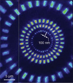
As nanotechnology progresses, improvements in nanoscale imaging tools are required to increase the resolution of nanometer-size features. To date, the best resolution of 15 nm is obtained by imaging with 1.52-nm wavelength soft-x-ray synchrotron radiation.1 However, more-compact and practical imaging systems are desired. To that end, researchers at the National Science Foundation Engineering Research Center for Extreme Ultraviolet Science and Technology at Colorado State University (Fort Collins, CO) and Lawrence Berkeley National Laboratory (Berkeley, CA), along with researchers at the P. N. Lebedev Physical Institute (Moscow, Russia) and the National Technical University (KhPI; Kharkov, Ukraine) have demonstrated, for what they believe to be the first time, nanometer-scale imaging with a compact, capillary-discharge pumped high-repetition-rate extreme-ultraviolet (EUV) laser.2 Spatial resolutions of 120 to 150 nm were achieved using the 46.9‑nm wavelength EUV source.
The imaging system consists of the compact laser, a scandium-silicon (Sc‑Si) multilayer-coated reflective condenser, a zone-plate objective, and a CCD detector. The condenser, the test-pattern sample to be imaged, and the objective are mounted on motorized translation stages inside a vacuum chamber connected to the source with standard vacuum fittings. The EUV source is a neon-like argon laser with 46.9‑nm wavelength, approximately 1.2-ns pulse duration, narrow spectral bandwidth (less than 10-4), high photon fluence, and good beam directionality. To prevent diffraction fringes and speckles in the image, sufficient photon flux is maintained while keeping the coherence low by equipping the laser with an 18-cm capillary-discharge tube that provides average pulse energy of approximately 0.1 mJ. The laser-beam profile in the far field has an annular shape with peak-to-peak divergence of about 4.6 mrad, with the laser operated at a 1-Hz repetition rate for most of the measurements. Beam diameter at the entrance of the microscope condenser is approximately 12 mm.
The Sc-Si Schwarzschild condenser with numerical aperture of 0.18 is composed of two mirrors, each with reflectivity of about 10% at 46.9 nm, resulting in total condenser throughput of approximately 1%-a parameter that could be greatly improved if high-reflectivity mirrors were used. This condenser produces a hollow cone of EUV light that illuminates the selected transmission sample, specially designed with circular patterns of small openings (see figure). Both the sample test pattern and the freestanding zone plate with outer zones of 200-nm lines are fabricated in a nickel foil using electron-beam lithography. With this EUV imaging system, the 100-nm sized features of the sample test pattern were clearly imaged.
High-average-power EUV
Using actual images from the EUV imaging system, spatial resolution was determined to be significantly better than 200 nm, with simulations indicating a resolution of 120 to 150 nm. “These results are the first demonstration of high-spatial-resolution imaging with a compact EUV laser. The key to achieving these results is a compact, high-average-power EUV laser developed at Colorado State University,” says researcher Georgiy Vaschenko. “Very high brightness of this source offers the advantages of obtaining high-resolution images with short exposures. The capillary-discharge EUV laser has the additional advantage of allowing the selection of the desired degree of spatial coherence, which can be controlled by adjusting the length of the capillary plasma column that produces the laser beam. The developed EUV microscope that can operate in both the transmission and reflection modes may find applications in imaging of material surfaces, semiconductor wafers, and other objects with nanometer-scale features.” In fact, the research team has just reported successful demonstration of high-resolution EUV imaging in reflection mode.3
The researchers are developing a new, sub-100-nm resolution EUV imaging system. This new system is expected to fit on a desktop and meet the requirements of compactness and versatility required for a commercial instrument. To further improve imaging resolution, the researchers plan to use a recently demonstrated high-repetition-rate tabletop nickel-like silver laser with a 13.9-nm wavelength to obtain sub-50-nm spatial resolution.
REFERENCES
1. W. Chao et al., Nature 435, 1210 (2005).
2. G. Vaschenko et al., Optics Lett. 30 (16) 2095 (Aug. 15, 2005).
3. F. Brizuela et al., Optics Express 13 (11) 3983 (May 30, 2005).
About the Author

Gail Overton
Senior Editor (2004-2020)
Gail has more than 30 years of engineering, marketing, product management, and editorial experience in the photonics and optical communications industry. Before joining the staff at Laser Focus World in 2004, she held many product management and product marketing roles in the fiber-optics industry, most notably at Hughes (El Segundo, CA), GTE Labs (Waltham, MA), Corning (Corning, NY), Photon Kinetics (Beaverton, OR), and Newport Corporation (Irvine, CA). During her marketing career, Gail published articles in WDM Solutions and Sensors magazine and traveled internationally to conduct product and sales training. Gail received her BS degree in physics, with an emphasis in optics, from San Diego State University in San Diego, CA in May 1986.
