IMAGE ENGINEERING: MICROSCOPE IMAGING: Using light for nanometric imaging
Nanometer-scale imaging is used in many applications, including inspection of integrated electronics and optics, materials research, biotechnology, and nanotechnology. In electronics, the features of interest can be only 50 nm across. For biological imaging, visible light can image features of a 1-µm bacterium and the larger viruses, but not features of an average protein, which can be 10 nm in diameter. Nanodevices—typically with sizes smaller than 100 nm—cannot be imaged using conventional far-field microscopy.
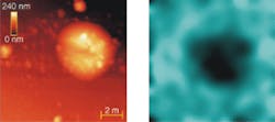
An ideal microscope would image these very small features nondestructively, in ambient conditions, and perhaps allow users to determine chemical composition as well as shape and size. Nonoptical imaging methods such as electron or force-probe microscopy are invaluable for research, but noninvasive optical systems take advantage of hundreds of years of accumulated experience in spectroscopy and contrast mechanisms (see Fig. 1). Near-field scanning optical microscopy (NSOM, SNOM, or just NOM) uses the properties of optical propagation close to a surface to retain optical imaging on a nanometric scale.
Near-field: a different ballgame
The basic difference between conventional and near-field optics is that instead of freely propagating waves, near-field optics deals with evanescent waves that decay exponentially away from the surface where they are generated. Evanescent waves are most familiar as the waves generated at the interface between glass and air when light is totally internally reflected. The electric and magnetic fields cannot be discontinuous at the interface—some of the field penetrates past the surface, although it falls off very quickly. A relatively strong evanescent field exists near the tip of an illuminating probe and near the tip of a scattering probe.
First systems
For the past 20 years, NSOM methods have been refined and variations explored. Today, NSOMs are commercially available, sometimes combined with other technologies. Myriad forms of near-field microscopy have been—and still are being—developed for specialized purposes, including nano-optics. NSOMs are being used to investigate the electromagnetic field distributions inside photonic crystals, subwavelength plasmon waveguides, and the like.
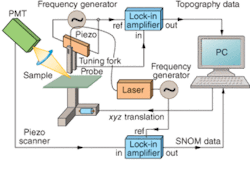
Although E.H. Synge proposed the concept of near-field imaging in 1928, practical devices weren’t realized until the 1980s.1 A typical system uses an optical probe with a subwavelength aperture at the tip. A probe is generally made from a tapered fiber coated with metal (usually aluminum) except for the aperture. Laser light is coupled into the fiber and the tip of the probe is brought to within a few nanometers of the sample. A control system based on a tuning fork can control the sample-to-probe distance to within 1‑nm. A small portion of the laser light exits the aperture and illuminates the sample. The area illuminated is roughly the same as the aperture size when the two are close together. Light transmitted by the sample is recorded by a photodetector in the far field.
An image is generated by raster-scanning the probe across the sample (or by scanning the sample below the probe). The resolution is on the order of either the aperture size or the distance from the sample, not the wavelength of the light used. The signal at the detector depends on the variation in the local complex dielectric constant with wavelength, the location in the sample plane, and the distance between the probe and sample.
Tips can be made smaller than 20 nm. But at smaller sizes, the EM field penetrates the metal coating and the metal coating heats up. The process of making reproducible tips continues to be an area of active research.
A near-field microscope can be operated using an aperture probe, scattering probe, or a fluorescent particle as the probe. The probe can be kept at constant distance from the sample surface, at a constant height, or it can be moved to generate a constant signal intensity.
The probe can act as an illuminator and as a detector in some cases. The important point is that the probe-to-sample distance must be much smaller than the wavelength used. Alternatively, the probe can act only as the detector, gathering emitted or reflected light from the sample—again, if both the distance and the aperture diameter are much smaller than the wavelength (see Fig. 2).A third option is to create a very small, very localized light source close to the sample—if the volume of the radiation source and the distance to the sample are much smaller than the wavelength (this is the mechanism of plasmon-aperture systems discussed later). Finally, some types of microscopy use light from the probe to create nonoptical effects in the sample (such as thermal, current, or sonic effects) and measure those outputs. Again, in this case, for effective resolutions the probe’s aperture and distance from the sample need to be much smaller than the wavelength.
If near-field illumination, and then far-field detection of scattered or reflected light is used, the image can contain artifacts. Only by using additional near-field detection through the same optical axis, explains Ludvig Balk of the University of Wuppertal (Germany), can such artifacts be avoided (see Fig. 3).No aperture
“Apertureless” systems use light-scattering probes. These are often a spherical metal particle attached to a transparent probe tip. When a laser beam is focused on the tip, local field enhancement creates a bright spot at the particle. A similar effect occurs at the tip of a sharp pointed metal or dielectric probe. When this “bright point” is scanned over the surface, an image can be formed with a resolution as fine as the tip.
Four advantages of scattering probes are that the incident laser power can be much higher than in aperture probes, the resolution can be finer, the wavelengths can vary from the visible into the microwave regime, and the probe can measure the physical topology of the sample at the same time it is generating a near-field image. The resolution depends again, not on wavelength, but on the sharpness of the probe’s tip. Because the instrument can be used in the infrared, it allows use of IR spectroscopy—which also provides information about chemical composition, crystallinity, and conductivity of the sample near the tip. The downside of scattering probes is that the sample is also exposed to the laser light, resulting in more background noise.
Electronics
Longer wavelengths into the terahertz region would be useful for measuring the conductivity of electronic circuits—as well as measuring conductivity of superconductors and organic conductors. A number of microscopy methods have already been developed for nanometric inspection of integrated electronics. Balk and an international group of coauthors recently presented a plenary conference talk on the subject that goes beyond the aperture and scattering-probe methods described above.2 Several methods discussed either are adapted to optical use or have always used optics but can resolve much finer details by using near-field optics. Optical-beam-induced currents (ONIC), for example, is a process that allows localized determination of space charge regions, defects, and local carrier diffusion length and lifetime. This process can be used for standard electronics and for examining local behavior in devices such as solar cells. If the sample is photoluminescent (PL), then near-field luminescence (NFPL) can be used: by illuminating the sample at a wavelength shorter than the PL wavelength one can measure the light emission locally (with either near-field illumination or near-field detection).
Another example of a nonoptical method that has been adapted to take advantage of the resolution of near-field optics is near-field cathodoluminescence (NFCL; shown in Fig. 1).3 The optical emission from materials such as gallium arsenide (GaAs) and diamond, when bombarded with high-energy electrons, provides a versatile and sensitive tool for analyzing the chemical and electronic properties of the light-emitting material. However, without near-field optics, the method had a resolution of, at best, a micron. A combination SEM/NSOM can lower resolution to 50 nm. Scanning photon-emission microscopy, which has about 2-µm resolution has also been adapted, as scanning near-field photon emission microscopy (SNPEM), with 300-nm resolution and single-photon sensitivity.
Bioimaging
A combination of scattering and aperture probes combines the benefits of both. A small finger grown onto the end of an aperture probe is covered in metal so as to leave the aperture at least partially clear (see Fig. 4).4 Reinhard Guckenberger and others at the Max-Planck-Institut für Biochemie (Martinsried, Germany) developed this arrangement for fluorescence sensing when a high background would be unacceptable. Its advantages stem from using a spatially fixed, contiguous source. “The resulting advantages are compactness of design, stability of the illumination, and reduced background,” they write. “The short distance from aperture to the tip might be essential for operation in an absorbing liquid.” Using this type of tip, the researchers imaged single fluorescent dye models, with details as small as 10 nm as well as providing information on their 3-D orientation.
Jordan Gerton at University of Utah (Salt Lake City) prefers to use a sharp silicon tip for fluorescence sensing. When metal gets too close to a fluorescing molecule, the excitation energy can transfer to the metal via a nonoptical process, quenching the fluorescence. Therefore, even though the metal-coated tips should provide a stronger enhancement to the applied optical field, nonmetal tips can yield images with higher signal-to-noise ratio. While in Stephen Quake’s group at Caltech (Pasadena, CA), he and colleagues developed a relatively simple technique to achieve 20-nm resolution. Commercial silicon probes modulate the fluorescence signal by oscillating above the sample surface. Subsequent demodulation strongly suppresses the fluorescence background. “One potential application,” he says, “is studying the dynamic interactions between biomolecules on the membrane of a single cell.”
Almost all of the applications for near-field microscopes seek to image ever-smaller features. Meanwhile, developing better tips and creating more practical instruments are still an engineering challenge. Nevertheless, having discovered a method for nanometric optical imaging, materials scientists and biology researchers are continuing to develop near-field methods.
FURTHER READING
Issue on near-field optics, J. Korean Physical Society 47 (96) (August 30, 2005).
Special issue on Nano-optics and near-field microscopy, Philosophical Trans.: Mathematical, Physical and Engineering Sciences 362 (1817), April 15, 2004.
REFERENCES
1. E.H. Philos. Mag. 6 356(1928).
2. L.J. Balk et al., Proc. SPIE 5856, 1 (June 2005).
3. E. Nogales et al., J. Appl. Phys. 92 (2) 976 (15 July 2002).
4. H.G. Frey et al., Appl. Phys. Lett. 81 (26) 5030 (Dec. 23, 2002).
Yvonne Carts-Powell | Freelance Writer
Yvonne Carts-Powell is a freelance writer living in Belmont, MA.


