OPTOELECTRONIC APPLICATIONS: MATERIALS PROCESSING - Excimers take more-refined approach to micromachining
Contrary to some perceptions, the excimer laser is not just the workhorse of the photolithography and vision-correction fields. Nor is it resigned to playing second fiddle to the increasingly popular diode-pumped solid-state laser for micromachining and other materials-processing applications. Given its unique ability to process a variety of materials with great precision and very little thermal effect—coupled with ongoing improvements in the design, efficiency, and cost of the laser—the excimer laser is expected to play a key role in the manufacture of microelectronics, medical devices, and consumer products for many years to come.
In particular, the excimer laser’s ability to deliver high pulse energies and high average powers at multiple UV wavelengths (157, 193, 248, 308, and 351 nm)—plus its inherent homogenous flat-top beam profile—make it a natural for a broad range of industrial applications, particularly those involving surface structuring, annealing, and step-and-repeat patterning. The excimer’s high pulse energy and M2 value allow larger areas of complex patterning to be machined using a mask projection technique, and the variety of excimer-laser wavelengths make it possible to customize the laser to the application, the dielectric, and the substrate; if trying to remove ITO from a glass substrate, for instance, and that substrate absorbs strongly at 248 nm, the laser can easily be tuned to 308 or 351 nm.
“The unique characteristics of the excimer laser mean that it is an inherently different laser in the way it is used for micromachining by mask projection imaging,” said Adrian Baughan, sales and marketing manager at Exitech (Oxford, England), which specializes in excimer-laser materials processing for display panels, solar panels, microelectronics, MEMS, and lithography. “DPSS lasers at short wavelengths rely on focusing the beam to a very small spot to create the high fluences required for machining, which is suitable for drilling, scribing, and cutting operations but not for selective removal of material over large areas. For micromachining applications that rely on the unique characteristics of the excimer laser, there is currently no known alternative.”
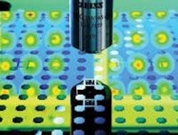
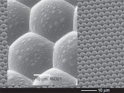
In addition, the low thermal effects are appealing for manufacturing applications involving nonmetals; when working with polymers and ceramics, the UV wavelengths are highly absorbed into the target material, resulting in very clean ablation with almost no collateral thermal damage (see Fig. 1). Excimer lasers can handle common plastics such as PEEK, PC, POM, polyimide, or PMMA with ease; as a result, other than photolithography, one of the most successful industrial applications for excimer lasers has been inkjet-nozzle drilling (see “Excimer lasers drill inkjet nozzles,” Laser Focus World, May 2002).“Any time you want to remove material over an area uniformly, you would want to use an excimer laser over a solid-state laser,” said Jim Higgins, director for excimer laser products at LightMachinery (Almonte, Ontario, Canada), a subsidiary of GSI Lumonics. “Excimer lasers are brilliant at doing large areas, and the absorption depth is about 0.3 of a micron in plastics.”
Broad application range
Over the past decade, other large-scale industrial applications of the excimer have included gauge-wire stripping for hard disk drives, ceramic chip capacitor marking, and wire marking. In addition, during the telecom heyday, the excimer emerged as the laser of choice for micromachining arrayed waveguides and fiber Bragg gratings.
“The excimer is suited to this application [fiber Bragg gratings] because the fiber is a transparent material, which means the interaction with a Nd:YAG or frequency-doubled laser is weak,” said Helmut Schillinger, head of the applications lab at TuiLaser (Munich, Germany). “To get interaction with transparent materials such as the fused silica fibers used in fiber Bragg gratings, you need deep-UV (248 and 193 nm); with other wavelengths, the light just passes through without doing anything.”
Excimer lasers are also good for large-area treatment of substrates or for imaging shapes onto various kinds of dielectric materials because they have a large-area beam that can be used to pattern features using a photomask. Numerous excimer-laser applications in microelectronics require the ability to project a demagnified image of a photomask onto the substrate to create a complex mark, to form MEMS structures, or to fabricate the substrate of thin-film-transistor (TFT) displays, for example. In fact, the annealing of thin silicon layers for flat-panel displays (FPDs) has emerged as another key industrial application for excimer lasers. To create the active element of FPDs, a thin layer of amorphous silicon is formed on a glass substrate in a vapor-deposition process. This layer must be transformed into polycrystalline silicon to yield the requisite electrical and photonic properties for high-resolution displays. Until a few years ago, this phase transformation was performed in high-temperature ovens (at 600°C), which required the use of expensive, thermally resistant glass. Today, virtually all flat-panel silicon annealing is carried out using 308-nm excimer lasers in combination with low-temperature ovens (200°C; see “Beam-shaping optics expand excimer-laser applications,” Laser Focus World, June 2005).
“The increasing density of the displays is driving this application, along with the ability to integrate on this polycrystalline not only the pixel drivers but surrounding driver circuits,” said Rainer Paetzel, director of marketing for Coherent Lambda Physik (Göttingen, Germany). “To make more sophisticated displays with systems on glass integrated into the glass, the silicon on the glass has to have the quality in terms of the polycrystalline structures, and this is where the excimer laser comes in.”
Cymer (San Diego, CA)—best known as the dominant supplier of UV laser systems for semiconductor manufacturing—and Carl Zeiss (Oberkochen, Germany) have formed a joint venture (TCZ) and developed a production tool for low-temperature polysilicon processes in TFT display production. Their first product is the TCZ 900X, a thin-beam crystallization system that combines Cymer’s 351-nm, 1000-W, 6-kHz excimer laser technology and proprietary two-chamber MOPA (Master Oscillator Power Amplifier) platform with Carl Zeiss’s optics and motion-control expertise.
“We conceived a new way of doing low-temp polysilicon,” said Brian Klene, president and CEO of TCZ and former executive vice president of emerging technologies and applications at Cymer. “A very long, ultrathin beam scans a glass panel, like a copier scans a sheet of paper. The nature of the beam means that a lot of power in the form of a high rep rate laser produces the most cost-effective solution.”
And despite the excimer’s maturity, the potential industrial applications for this laser are by no means saturated. According to Paetzel, a number of new high-power techniques are moving into the commercial realm.
“A quite promising area is where the excimer laser is used to treat the cylinder wall of diesel engines to improve lubrication and enable cleaner combustion by ablating the cast iron surface to create a microhydrodynamic structure in the graphite,” he explained (see “Targeting diesel engine efficiency,” Industrial Laser Solutions, October 2004). “Major automakers such as Audi are applying this technique on the production floor, and the excimer is the only laser that can deliver the necessary power and reliability.”
Smaller laser, bigger market
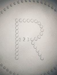
In addition, the advent of increasingly sophisticated lower-cost, low-power (10 W) excimer lasers that incorporate advances in optics and thermal management gained through the investments made in high-end excimer lasers (used in semiconductor manufacturing) is opening up new opportunities in niche materials-processing applications such as micromarking lenses for eyeglasses, microencoding diamonds for jewelry, and microetching sapphire for chip manufacturing (see Fig. 2).At TuiLaser, for example, the company’s compact high-average-power excimers originally made a splash in the vision-correction and telecom markets because of their high average powers (10 mJ at 193 nm, 15-20 mJ at 248 nm) and high rep rates (in the multikilohertz range). Today, while fiber Bragg gratings still represent a market for TuiLaser, 80% of the company’s business is in LASIK, telecom inspection, and materials processing, such as marking glass, gemstones, and exotic materials ranging from sapphire to lithium niobate and lithium tintobate.
“We adapted and moved some of the technologies known in the high-end systems into the less expensive compact excimers, such as special procedures to get very good gas lifetimes and optics lifetimes,” Schillinger said. “Some of the very advanced materials and the cost for these materials came from the companies in the lithography market, and with our strategic partnership with Coherent Lambda Physik some of these technologies are now becoming available on the smaller systems.”
This, in turn, has enabled the introduction of compact excimers into niche applications such as mask writing, mask inspection, direct-write chip production, and nanomanufacturing (see photo). For example, according to Schillinger, nanoapplications such as pulsed laser deposition are being driven by the excimer because it is the best for generating complex mixtures of materials for superconductors and for creating layers for high-density hard drives.
Schillinger also believes the technical advances in excimer lasers coming out of the semiconductor field will keep the excimer competitive in other industrial applications by reducing maintenance costs and increasing lifetimes and reliability. Changing the materials that the excimer laser is made from to eliminate anything organic, for instance, means the gas in the laser is now less than 10% of the overall maintenance cost, according to Higgins.
“The price pressure will continue to be an issue, even with the DPSS systems coming in,” Schillinger said. “We will leverage our technologies from the high-end excimer systems and transfer technology to the compact systems to produce cheaper light. People have said for a while that the excimer cannot withstand the onslaught from the DPSS lasers, but we are keeping up quite nicely.”
About the Author
Kathy Kincade
Contributing Editor
Kathy Kincade is the founding editor of BioOptics World and a veteran reporter on optical technologies for biomedicine. She also served as the editor-in-chief of DrBicuspid.com, a web portal for dental professionals.


