Diamond cools high-power emitters
Heat spreaders are essential for cooling high-power laser diodes. With its high thermal conductivity, diamond has joined the ranks of other dielectrics and metal composites as a practical material for heat spreaders.
The demand for higher optical output from high-power pump lasers requires efficient thermal management because laser output drops drastically with increasing chip temperature. Thermal management of pump lasers critically affects laser wavelength, output power, threshold current, slope efficiency, and operating lifetime. For example, lasing wavelength shifts by about 0.3 nm/K for 980-nm pump lasers. The maximum optical power is limited by thermal rollover, while the power coupled into an optical fiber is limited by kink, which is caused by local heating in the active region of the laser chip. The threshold current of a pump laser increases while the slope efficiency decreases exponentially with the junction temperature. For these reasons, thermal management of pump lasers is crucial to device performance and extended long-term reliability.
Heat spreaders and heat sinks
Heat can be dissipated in two steps-first by spreading heat out, and then by sinking it away. A heat spreader is not unlike a water hose; it transmits heat (akin to dispensing water) and is described in terms of thermal conductivity. A heat sink is similar to a reservoir; it stores heat (akin to holding water) and is described in terms of heat capacity. A heat spreader does not retain heat, so it requires a combination of high thermal diffusivity and low heat capacity. In contrast, a heat sink needs high thermal diffusivity and high heat capacity.
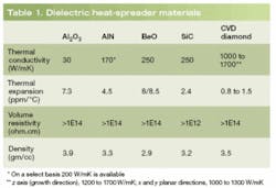
Many materials are used in semiconductor and photonic packaging, each with its associated positive and negative characteristics. Metals have a high concentration of electrons and their thermal conductivity is dominated by electrons. For nonmetallic materials, in which electrons are not available for thermal conduction, thermal transport typically occurs through phonons (for example, in diamond). Many applications require both electrical isolation (dielectric-based heat spreaders) and thermal conduction. Dielectric heat spreaders are ideal for laser diodes and all semiconductor integrated circuits (see Table 1).
The rapidly increasing demand for laser-diode submounts with heat spreaders having high volume resistivity (z-axis isolation) is being driven by the requirement of populating the top side with fine-linewidth circuit patterns that accommodate active and passive chip devices (for example, thermistors, polarity-protection diodes, and photodiodes).
Sizing of heat spreaders on dielectric materials
Our experience suggests a rule of thumb that the thickness of a heat spreader should be approximately a quarter to a half of the lateral chip dimension. If the spreader is too thick, its performance is not significantly improved because the additional thickness adds more thermal resistance. If it is too thin, there is insufficient material to spread the heat laterally away from the source.
Typical lateral dimensions for heat spreaders are approximately five times the dimension of the heat-source device for centrally mounted chips, and approximately 2.5 times the device dimension for edge-mounted chips. A separate computer-model evaluation for diamond with a laser diode as a point source of heat suggests an optimal thickness-to-area ratio of 1:4. In both cases, the heat spreader is mounted to a copper (Cu) block with 10 times the chip dimensions.
It is important to note that the components of a laser-diode/heat-spreader/Cu-block assembly are poorly matched for coefficient of thermal expansion (CTE) and will result in serious device stresses. An alternate approach is the use of metal-matrix composites and alloys (the term “composite” will be used here to describe two or more materials bonded together).
Thermal properties of metal composites
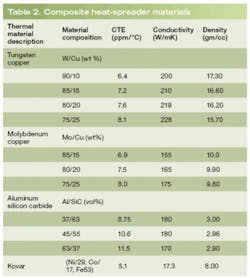
Conventional materials for heat spreaders include the so-called refractory metals, such as tungsten (W), molybdenum (Mo), tantalum (Ta), and so on. The primary combinations are CuW and CuMo. Historically, CuW is the leading material for CTE-matched thermal management. The refractory metal typically constitutes 60% to 90% of the composite, which imparts the lowered CTE but reduces the thermal conductivity to less than a half of that for Cu alone (see Table 2). When the source of heat is a point source (laser diodes of about 0.25 × 0.25 mm in size are common), the reduced thermal conductivities of composites are unsuitable. When the primary objective is to spread heat rather than match CTE, the composites do not compare to some of the dielectric heat spreaders. In addition, the density of metal-composite materials are typically three to five times heavier than their dielectric counterparts-a factor to be considered in airborne and space applications.
Dielectric heat-spreader materials are better suited than metal composites for attachment to silicon (Si), gallium arsenide (GaAs), indium phosphide (InP), indium gallium arsenide (InGaAs), and so on. Cost, weight, conductivity, and fabrication complexities of composites relegate their application to those with moderate power densities.
CTE and heat-spreader performance
If we assume that the semiconductor die is attached to the heat spreader by solder (mandatory in applications of greater than 1 W), then the CTE of the spreader must closely match the CTE of the semiconductor material. The die/solder/spreader is a rigid, monolithic assembly that can encounter temperature excursions of greater than 100°C in some applications.
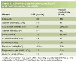
Texas Instruments (Dallas, TX) created and patented two-metal composites called Silvar and Silvar-K that allow matching of the CTEs of low-power GaAs devices. This development is an example of the current CTE-matching requirements for a variety of semiconductor materials (see Table 3). Mounting the GaAs die in a compressive state by selection of a heat spreader having a CTE in the range of 6 to 9 ppm/°C is the prevailing design methodology.
Applicability of diamond to heat spreaders
Diamond has the highest heat conductivity of any material. Diamond films can be readily deposited by chemical-vapor deposition (CVD). The majority of diamond films reported to date have been grown on Si wafers, primarily because of availability, low cost, and material characteristics. Crystal growth at the Si nucleation surface (800°C to 1100°C substrate temperature) is exposed to a plasma of hydrogen and a carbon-containing reagent such as methane. The ionized hydrogen first attaches to the substrate, then combines with the methane radicals, leaving behind diamond, diamond-like carbon (DLC), and graphite crystals.
Crystal growth at the nucleation surface occurs first by the accumulation of DLC crystals, then by growth in the planar direction, and finally by epitaxial growth of the film normal to the substrate plane (z axis). This results in much smaller grain sizes and smaller spaces between the grains on the nucleation side of the diamond film and larger grains and fewer, yet larger, spaces between the crystals on the growth side. Such a coarsening effect results in a columnar crystal structure of crystals; the thicker the film, the coarser the diamond grains on the top.
The surface finish on the growth side is typically estimated at 5% of the film thickness, while the finish of nucleation side is that of the Si wafer. Polishing the growth side is slow and costly. Although grain boundaries are a major impediment for semiconductor fabrication, they are only a slight problem for heat-spreader applications. The thermal path is impeded less by grain boundaries along the growth direction (z axis) and is impeded most in the x and y directions.
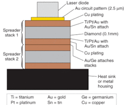
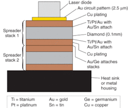
In 2003, James Sung of Kinik Co. (Taipei, Taiwan) provided comparative data on computer-chip cooling for diamond versus ceramic. The thickness of the chip and spreader were specified, but not length and width. A constant 110°C junction temperature was chosen for illustration purposes. The data showed that a 1.0-mm-thick alumina spreader was able to dissipate 21 W, while a 1.0-mm-thick beryllium oxide spreader handled 39 W. In comparison, a 0.15-mm-thick CVD diamond spreader could handle 83 W, while a 1.0-mm-thick CVD-diamond version handled 160 W. Such qualities have inspired the design of a diamond-based heat spreader (see figure, p. 159).
The downside of CVD-diamond heat spreaders is their low CTE. The semiconductor device must be maintained in a compressive state at all times; temperature excursions of the device due to ambient temperature variations, high-rate modulation, or continuous-wave operation will affect its long-term reliability.
The printed-circuit-board industry commonly uses copper-Invar-copper (CIC) stacks to control the expansion ratio of multilayers. The CIC composite stack has proportional thicknesses of 20% Cu, 60% Invar, and 20% Cu, which results in a CTE of 5.2 ppm/°C. The sandwich concept is being evaluated for applicability to diamond heat spreaders.
Cost will drop
Dielectric materials provide much flexibility in a wide variety of high-power head-spreader applications, but CVD diamond is the ultimate heat-spreader material. A “tunable” CTE is currently not available; however, experiments are under way to ascertain adhesion characteristics of various metals to the polished surface, as well as dielectric stresses associated with thick Cu and gold plating. Very high-volume applications in numerous industries will reduce the cost per square inch by a factor of three or four by late 2005. Performance applications will dominate in the immediate future.
ROBERT QUAGANis president of Ion Beam Milling, 1000 E. Industrial Park Drive, Manchester, NH 03109; e-mail: [email protected].