As a material system that offers compatibility with the currently ubiquitous microelectronic technology, silicon offers a highly attractive option for materials researchers seeking to design micro- and nanophotonic building blocks for future generations of photonic integrated circuits. At a symposium on new materials for microphotonics held during the Spring 2004 meeting of the Materials Research Society (Warrendale, PA), April 12–16 in San Francisco, CA, several presenters focused on the state of the art in silicon.
During the first half of an opening tutorial session on photonic micro- and nanostructures, Albert Polman, a leading researcher in the effort to make a silicon laser, referred to a recently published projection for growth of optical circuitry in computer systems from today's optical connections between computers to optical connections between circuit boards within computers within the next two to five years; to chip-to-chip connections in five to ten years; and possibly to on-chip subsystem interconnects in 15 or more years.
While the ultimate feasibility of on-chip optical interconnects is controversial, the idea remains attractive. "For instance, Intel might like to have an optical clock distribution, because more than 50% of the energy loss on a chip is due to heat dissipation in the wires," said Polman, who heads the optoelectronics materials department at the FOM-Institute for Atomic and Molecular Physics (Amsterdam, The Netherlands).
Guiding optical signals around increasingly tight corners in these small structures will require building micron-scale optical components out of high-index-of-refraction and photonic-bandgap materials that can act as effective waveguides and resonators on that scale. Silicon waveguides offer bending radii on the order of 1 µm, although they can be plagued by scattering losses, while photonic crystals offer very tight turning radii that are much less material dependent. Polman emphasized the potential optimization of functionality to be obtained through photonic-crystal integration on silicon.
In terms of active photonic components, however, a longstanding drawback in developing silicon-based devices has been the relative inefficiency of light emission via the indirect bandgap structure of bulk silicon. Significant research activity has gone into this problem over the last decade, and doping of silicon nanocrystals with rare-earth elements such as erbium presents one of the most promising potential solutions. "It would be great to dope silicon with erbium to get an erbium-doped silicon laser or light-emitting diode," Polman said. "The first erbium-doped silicon was made about 20 years ago, but there is still no laser."
The main problem with putting erbium in silicon is that erbium is also electrically active, he added, which leads to an Auger process in which the free carriers quench the excited erbium. But the inhomogeneous structure of nanocrystalline silicon enables "complex couplings and interactions" between free carriers, bound carriers, and rare-earth ions, according to Se-Young So of the Korean Advanced Institute of Science and Technology (KAIST; Daejeon, Republic of Korea), who described the simultaneous excitation of multiple species of rare-earth ions to obtain broadband IR luminescence. And based on heat-induced effects observed after an ion implantation process for erbium doping of nanocrystalline silicon at the National Institute for the Physics of Matter (INFM) and the University of Catania (Catania, Italy), Domenico Pacifici reported that amorphous silicon may provide a photoluminescence efficiency similar to that obtained with nanocrystalline silicon.
A real silicon-based laser
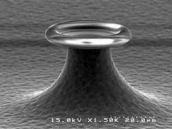
Actual microphotonic silicon devices discussed at the meeting included a 40-µm-diameter toroidal microlaser fabricated using standard silicon CMOS technology and emitting at 1.5 µm, developed by Polman's group in Amsterdam in collaboration with researchers at the California Institute of Technology (Cal Tech, Pasadena, CA); and a silicon-nanocrystal optical modulator, developed by Cal Tech and Intel (Santa Clara, CA) researchers, which actually makes use of the Auger quenching process that limits the photoluminescence efficiency of erbium-doped silicon (see figure).
A recently demonstrated erbium-implanted-silica toroidal microcavity laser on silicon (seen here in a scanning-electron micrograph) may open up a new field of microresonator science and technology, says Albert Polman. "For example, silicon-based microresonators can now be implanted with other rare-earth ions to fabricate lasers that operate in the visible, with noble metals to form nanocrystals with well-defined surface plasmon resonances and associated nonlinear properties, and with silicon quantum dots that can serve as sensitizers for erbium or may show lasing in the near-IR." ( FOM-INSTITUTE AND CAL TECH)
The Amsterdam and Cal Tech groups also presented a joint paper that proposed solving the quenching limitations of erbium-doped silicon by using plasmonic waveguides formed at the interface between a metal (silver) and a dielectric (silica). They described a design methodology that could potentially enable "the integration of optical and plasmon phenomena in microphotonic integrated circuits." As a potential vehicle for creation of optical nanostructures operating below the diffraction limit, plasmonics also provided a major area of focus in the symposium on microphotonics.
The conference, which this year hosted about 2700 paid attendees along with about 300 exhibitors and others, included a broad range of photonics topics. Among these, a symposium on amorphous and nanocrystalline silicon science and technology explored new developments in solar-cell technology, and a symposium on materials and device technology for flexible electronics focused to a large degree on optical light-emitting devices.
In spite of the esoteric scientific focus that pervades discussions of new and emerging developments in these fields, the close juxtaposition of research goals to major and often commercial applications can render a level of excitement similar to what one might expect to hear in a Las Vegas casino. "In terms of trying to achieve a silicon nanocrystal laser, many people are active in this field because we feel it cannot be missed," Polman said. "We are so close."

