Surface-mount photonics simplifies optical assembly
Novel assembly and packaging techniques used for optoelectronic devices benefit from existing electronics production processes and promise lower-cost precision single-mode optical components.
Optical assemblies produced with the surface-mount-photonics process look more like semiconductor products than optical products. That's no accident. The overarching design-for-manufacturability objective for the optical assembly and packaging process recently developed by Xponent is to enable leading-edge optical components to be assembled with the low-cost processes used to assemble electronics devices. In production, surface-mount-photonics (SMP) components go through three stages of manufacturing and assembly, all of which take advantage of established processes originally developed by the semiconductor industry. These stages are chip production, optical assembly, and packaging.
Chip production
In the first phase, SMP device chips are produced by adapting standard device types—such as edge-emitting lasers (Fabry-Perot and distributed feedback devices, for example), p-i-n detectors, and thin-film filters—using wafer-level processes such as lithography, precision etching, and deposition. During SMP chip production, precision alignments, and coupling features are put in place thousands at a time with submicron, wafer-level semiconductor processes to allow simplified, low-precision assembly throughout the subsequent assembly. Surface-mount-photonic laser facets, for example, are etched and coated on the wafer. A surface-mount coupler (SMC) is then deposited in front of the laser facet (still on the wafer). The SMC efficiently couples light into a matching single-mode waveguide in the planar lightwave circuit (PLC) with less than 0.3-dB loss and relaxes alignment tolerances by a factor of 10 from ±0.2 µm to ±2 µm.1
The SMP active devices, such as lasers and detectors, are fully functional and can be tested on the wafer, eliminating the need for bar- or chip-level testing and interim submount packaging. Good SMP die are electronically "mapped" on the wafer, then an automated visual inspection is performed before singulation. The known good die are placed into gel packs ready for presentation to a bonder for flip-chip assembly.
Optical assembly
After chip production, the SMP device chips are bonded to a PLC substrate chip with interconnecting waveguides to form an optical assembly. From the point of view of the bonder, all SMP chips look the same. One of the design-for-manufacturability criteria for SMP device chips (lasers, filters, detectors, and so on) is that the minimum critical alignment window for bonding to the PLC is ±2 µm to allow the optical alignment to be done passively. The devices do not need to be turned on and actively monitored to ensure adequate alignment, as is typically the case with most single-mode optical assemblies.
Furthermore, unlike the standard free-space optics assemblies, the SMP optical train is fully enclosed within the bonded chipset and does not cross free-space. Hence the assembly does not need to be put in a hermetic package, which is a significant cost saver. Instead, devices are designed to be insensitive to ambient conditions and require only a simple encapsulant coating for final protection of the assembly.
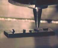
FIGURE 1. A triplexer assembly—used in bidirectional passive-optical-network applications—has just been assembled by a eutectic die bonder. All six bonded chips—a laser, a monitor photodiode, a video-receiver photodiode, a data-receiver photodiode, and two filters—are soldered to a PLC substrate with connecting waveguides and electrical contact pads. In this bonding step, the mechanical and optical attach, the alignment, electrical connections and the thermal path are all completed with one low-cost process.
Surface-mount-photonic lasers are designed with co-sided p and n contacts that are bonded to contact pads on the PLC. The heat path—described in more detail later—is also connected in the bonding step. Thus, in a single low-cost bonding process the optical and mechanical attach, alignment, electrical connections, and the thermal path are completed (see Fig. 1).
Final packaging
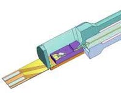
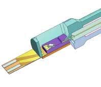
In the final phase, the SMP assemblies are placed into packages with a fiber interface (pigtail or receptacle) and electrical leads. As noted previously, SMP assemblies do not need to be hermetically sealed. Therefore a low-cost, injection-molded plastic clamshell package is used. The precision plastic used in this housing has designed-in features that align the fiber-stub ferrules and lead-frame carriers to simplify assembly. The terminating waveguides in the PLC are mode-matched to the fiber core and are terminated into a V-groove that is ready for fiber placement. In the final packaging step, the fiber tip is aligned in the V-groove within a 20-µm window. An index-matching epoxy is applied between the fiber tip and the edge of the waveguide to complete the optical train (see Fig. 2). Wirebonding, flip-chip bonding, and epoxy dispense and cure are the processes required for the packaging stage. Standard widespread low-precision electronics assembly equipment is used to perform these steps—no traditional optical-specific assembly and packaging equipment is needed.
Traditional assembly and packaging
The SMP assembly and packaging sequence described is much simpler than that normally used for single-mode lasers. A typical edge-emitting laser would have its facets defined by cleaving the wafer into bars. Facet coating and test typically occur at the bar level. In many cases, chips then go through an interim packaging step to place them on submounts for test and burn-in before final packaging.
Once traditional single-mode laser chips are on submounts, submicron alignment tolerances must be met to get the laser light into a fiber through various lensing options. These alignment tolerances require the use of an active laser welder in which the laser is turned on, the coupled signal is measured, and the alignment is adjusted to actively optimize coupling before welding. Many assemblies require annealing to conduct post-weld shift correction.2
Because the signal propagates through free space and the laser facet is exposed to the ambient environment, a hermetic package is required to protect the optical train. Hermetic package assembly demands vacuum evacuation, bake out, inert and tracer gas fill, welding/seam sealing, and gross and fine leak testing of the package. In addition to this processing, the hermetic packages themselves tend to be expensive. They are generally controlled-expansion alloy metals with gold plating and glass to metal feedthroughs for leads.
Performance over temperature
The structural and optical design of surface-mount-photonics components also has some advantages for thermal performance. Heat generated by the lasers must have an efficient path out of the package. In the case of an SMP laser, the active region of the laser is directly bonded to silicon (see Fig. 3). With a thermal conductivity of 168 W/mK, the silicon acts as a direct heat sink and spreader from the active region. The heat then travels through a carrier substrate. The bottom-side of this carrier can be exposed through an opening in the plastic housing to provide direct access for further spreading.
Another feature of SMP assemblies that enhances performance over temperature are etched facets. The etching of facets enables optimization of the laser cavity size. Of particular advantage is the ability to have smaller cavities than are typically achievable through a cleaving process—this allows for greater flexibility in the optimization of speed, temperature, and power performance (see Fig. 4).
Reliability
One final area of critical concern and effort is reliability. Any new assembly and packaging process must pass this hurdle before being accepted by the industry. Several features of the SMP process benefit reliability performance. First is the overall increase in alignment tolerances and greatly reduced coupling lengths. An assembly that comes together with ±2-µm alignments combined with reduced optomechanical leverage is inherently more forgiving than one that requires submicron alignments. Mechanical shock and vibration, aging, and temperature cycling are all more likely to adversely affect the more precisely aligned assembly.
Second, the chip-level SMP processing of lasers also benefits their reliability. The deposition of the surface-mount coupler has a secondary benefit of passivating and protecting the facet. Exposed facets are subject to degradation from strong field interactions with the ambient environment that can lead to galvanic corrosion and electromigration. In an SMP laser chip, the facet is buried under a dielectric that acts as a protective coating. The lack of exposure of the optical train to the ambient environment is an advantage for the entire SMP assembly but in particular for the lasers.
Third, although nonhermetic packages reduce manufacturing costs, they also have secondary reliability benefits. With no need for leak-proofing, failure modes from leaks are eliminated. In a butterfly package there are more than a dozen joints between leads and the package casing that are all candidates for leakage-induced failures. Early surface-mount-photonics reliability tests validate these advantages. Both SMP Fabry-Perot lasers and SMP p-i-n diodes have exhibited very stable performance over thousands of hours of testing. To date, over 380,000 real-time hours have been logged for the lasers, with no observed failures with many devices biased at maximum rated operating current up to 100°C. Surface-mount- photonic photodiode chips have completed full Telcordia GR468 qualification including 5000-h accelerated aging under bias at 175°C.
Traditional optical assembly and packaging drive significant costs across the industry. For this reason the overheads associated with time-consuming serial processes and expensive optical-only equipment have been addressed from many angles—eliminating as many optical-only processes as possible is the ultimate goal. Almost all optical devices end up next to semiconductors in the final products so the convergence of optical assembly and packaging with the already lower-cost electronics infrastructure reduces the cost of optical devices while also driving cost savings throughout the consolidated supply chain.
REFERENCES
- D. Vernooy et al, IEEE Photon. Tech. Lett. 16(1) (January 2004).
- See laser welding process and cycletime description AMS4200 Laser Welding Workstation, Newport, www.newport.com.


