Arrays of optical sensors are used for various purposes at wavelengths ranging from x-ray to the IR. As ever-more-demanding applications push pixel size down and the total number of pixels up, demands on the sensor signal-processing electronics also rise. Traditionally, these electronics have been placed a distance away from the arrays themselves to reduce thermal loads or physical size of the array package or improve other characteristics. The faster and larger the array, however, the more important it is to have the electronics close by; smaller pixels produce smaller signals that can get swamped in noise arising from too-long connections.
One way to bring electronics and sensors together is with 3-D stacked electronic structures, which greatly reduce the size of the electronic package. High-density-interconnect (HDI) technology, developed about a decade ago, is expensive and has been used in military and aerospace applications; in HDI, ceramic substrates containing integrated-circuit (IC) chips are layered together with many interconnect layers. Yield problems as well as expense have limited HDI to high-end use.
Researchers at GE Global Research (Niskayuna, NY), Los Alamos National Laboratory (Los Alamos, NM), and the Air Force Research Laboratory (Albuquerque, NM) have developed a lower-cost alternative to HDI called chip-on-flex (COF) that promises to bring the extremely small packaging capabilities of 3-D stacking to the everyday world.
At the heart of a COF assembly are 25-µm-thick polyimide films that hold both IC chips and interconnects. First, interconnect metal is deposited on one or both sides of the film, and then patterned and sprayed with adhesive. A flip-chip pick-and-place apparatus then positions IC chips to a 12-µm accuracy; the polyimide film and chips are subsequently encapsulated in epoxy, creating a 1- to 2-mm-thick carrier. Further metallization, photolithographic patterning, and etching connect the chips to the interconnects. Taking advantage of economies of scale, a single large chip carrier can be fabricated and then sawed into smaller unit carriers.
Thinning is key
A 3-D COI assembly is fabricated by gluing many carriers together in a stack. To create a truly dense assembly, the carriers are drastically thinned by mechanical grinding before stacking.
"Generally, the molding material is ground off first," explains Raymond Fillion, from GE Global Research. "If the die are thicker than the desired module thickness, then the grinding process will continue into the chip's back side. Chip thickness varies by device type and manufacturer. Silicon devices that are not thinned at wafer level can range from 250 µm to more than 700 µm. If a module needs to be thinned to 200 µm, the silicon chip is 500 µm thick, and there is 50 µm of polymer interconnect structure on the chip surface, the thinning process will thin the chip to about 150 µm." The researchers have thinned the carriers to as small as 100 µm, with the chips thinned to an even scanter 50 µm.
Rather than creating a "horizontal" stack, in which the top surface of the stack serves as the interface to the sensor array (and all interconnects must pass to the array via the edge of a single top layer), the researchers chose a "vertical" arrangement, in which one side of the stack interfaces with the array. In this way, input/output (I/O) connections—which naturally terminate on the side of the stack—are easier to interface with the array. In addition, many layers rather than one route the I/O connections to the array, making the connections much wider and easier to fabricate.
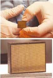
In one example, the targeted device was an 8000-pixel, 16 × 20-mm sensor array. For test purposes, the array was silicon; in reality, it could be one of many semiconductors, depending on the wavelength (for example, mercury cadmium telluride for the mid-IR). One requirement was that the 3-D stack not be larger than the footprint of the array sensor. To fabricate the cube, 50 carriers were attached together in a custom jig, forming a stack with adhesive films between them. The side edges of the cube were ground to flatten them and expose the I/O connections.
Further steps, including laminations, metallizing and etching, and fabrication of conductive bumps for connecting to the sensor array, result in the finished cube (see figure). A similar pattern of conducting bumps on the array allows the array and cube to be electrically connected together.
Five cubes were fabricated, with all showing a less than 100% connection; the failures were at the corners of the cube and were attributed by the researchers to nonplanar surfaces and a low cure temperature for the polymeric adhesive used—problems solvable in the future. All 2-D and 3-D connections within the cube itself had a 100% yield, however.

