Low-temperature bonding makes cheaper optoelectronic circuits
Engineers at IESL-FORTH and University of Crete (Heraklion, Greece), the Max Planck Institute of Microstructure Physics (Halle, Germany), and the Institute of Microelectronics, NCR Demokritos (Athens, Greece) have developed a process that allows standard silicon (Si) integrated circuits to be combined with gallium arsenide (GaAs) optical devices, but without the disadvantages of flip-chip bonding or trying to grow III-V devices on silicon. The technique initially works at low temperature, yet produces a strong bond between the GaAs and Si chips and causes relatively little degradation to the performance of either kind of circuitry. Crucially, it uses processes that are compatible with commercial complementary metal-oxide semiconductor (CMOS) technology. Researchers say that, with some improvement, the technique should allow hybrid chips to be fabricated with a process flow that is almost as straightforward as that for a standard monolithically integrated chip.
The new technique is necessary partly because flip-chip bonding—in which two chips are bonded back-to-back—is difficult and thus expensive. Also, though optoelectronic circuits have been grown monolithically on top of silicon, the performance of the circuits produced in this way tends to be degraded due to the poor quality of III-V materials deposited. This is caused, in part, by the mismatch between the crystalline structures of the two materials.
The process developed is based on commercial bipolar CMOS (BiCMOS) technology.1 As with the flip-chip method, the new technique involves three main steps to manufacture the hybrid circuits: the fabrication of the two chips, and their bonding. First, the BiCMOS circuitry is grown in the normal way on a silicon wafer, then it is covered with silicon dioxide—deposited using low-temperature plasma-enhanced chemical vapor deposition—which is subsequently polished until the surface is flat (planarized). This layer is then covered with spin-on glass to remove any remaining imperfections. In the meantime, the optoelectronic devices are fabricated on a GaAs wafer that has been coated with an etch-stop layer. Apart from the fact that their structures are inverted—so that the devices that would normally be at the top of the chip are now buried—they are grown in the normal way.
The final stage, the bonding, first involves baking the silicon chip to remove any volatile elements. Next the chips are aligned, bonded, and the bond strengthened via a low-temperature (200°C) annealing step. Now, the GaAs substrate can be removed using fast wet etching (which leaves the chip almost entirely strain-free at room temperature), and the etch stop removed with hydrofluoric acid to expose the optoelectronic devices. At this stage, low-temperature processing is no longer important. Free of the GaAs substrates, the difference in the thermal coefficients between the two material systems may cause some deformation of the optoelectronic circuitry, but not damage. Thus, the temperature is allowed to rise to 400°C, improving the bond further. Finally, any remaining optoelectronic layers can be deposited on the chip, vias can be opened and electrical interconnections deposited.
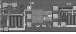
The feasibility of the new technique has been demonstrated by fabricating an optical link on top of both processed and unprocessed silicon wafers (see figure). Though high-frequency characterization of the optoelectronic circuits has yet to be carried out, the performance of both the optoelectronic and electronic devices seems to be unaffected by the bonding process. However, where BiCMOS circuitry is present, it does seem to affect the yield of the subsequent GaAs processes. Researchers say they are currently examining a number of possible solutions to this problem.
In other ways, however, the process has proven robust. For instance, 90% of the surface was deemed adequately bonded after annealing at 200∞C under some pressure. In addition, no voids (gas bubbles) were created by the bonding process. Further progress with the planarization of the Si wafer should, they say, make the process even more valuable.
REFERENCE
- A. Geourakilas et al., Appl. Phys. Lett. 81(27), 5099 (Dec. 30, 2002).
About the Author
Sunny Bains
Contributing Editor
Sunny Bains is a contributing editor for Laser Focus World and a technical journalist based in London, England.
