III-nitrides show promise for telecom wavelengths
Recognized as technologically important materials for optoelectronics, III-nitride wide-bandgap semiconductors are used in light-emitting diodes (LEDs) with emission wavelengths from the ultraviolet to amber, and blue/UV-emitting laser diodes.1 These materials are excellent for photonic devices because of their large energy bandgaps, their highly efficient light emission, and their ability to be bandgap engineered through the use of alloying and heterojunctions. Recent advances have shown that nitrides are also promising materials for optical communications at 1.55 µm. The .continuous variation of the refractive index (n) of AlxGa1-xN with x, from n = 2.34 (x = 0) to n = 2.03 (x = 1) at 1.55 µm makes III-nitrides ideal candidates for optical waveguide devices.2
The III-nitrides are potentially superior to indium phosphide (InP)-based alloys because of their better index match with silica optical fibers. Also it may be feasible to fabricate erbium-doped III-nitride waveguide optical amplifiers, which would lead to the integration with other functional optical devices, such as optical switches, wavelength routers, light sources, and detectors. The large conduction-band offset in the aluminum nitride/gallium nitride (AlN/GaN) heterostructure (approximately 1.9 eV) may allow the realization of intersubband emitters and detectors operating at 1.55 µm.
In addition, recent experimental results indicate that the band edge emissions in InN coincide well with the optical communications wavelength at 1.55 µm. Because of their intrinsic robust physical properties, III-nitride-based devices can operate at higher voltages and power levels, and in harsher environments than conventional III-V semiconductors. These characteristics are crucial advantages for optical communications applications.
Intersubband transitions
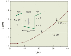
The intersubband transitions in AlGaN/GaN quantum wells (QWs) can be tailored to 1.55 µm. Such QW devices have distinct advantages compared to those based on other materials, including large electron effective mass and longitudinal optical phonon energy. These properties are crucial for the ultrafast intersubband relaxation of electrons. Optical absorption lines between n = 1 and n = 2 subbands in AlGaN/GaN QWs have been observed by several groups in structures grown by molecular beam epitaxy (MBE) and metal organic chemical-vapor deposition (MOCVD).3–5 With improvements of AlN epilayer quality, we have recently grown AlN/GaN QWs by MOCVD that emit light near 1 µm corresponding to the intersubband transitions in wells 20 Å wide.6 By changing the well width and material (AlGaN), the transition wavelength of the intersubband transitions can easily be tuned from 1.3 to 1.6 µm (see Fig. 1).
Photonic integrated circuits
Silica-based photonic integrated circuits (PICs) have become a popular approach for wavelength-division multiplexing and demultiplexing. Because silica is not a semiconductor, such PICs can only be tuned slowly using thermal effects. Indium phosphide–based PICs are quickly tunable with carrier injection or by application of an electric field. However, because of its high refractive index (n = 3.2), high temperature sensitivity and high insertion loss, InP-based PICs are not yet commercially competitive.
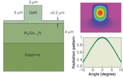
The possibility of developing new PICs based on III-nitride semiconductors for fiberoptic communications is being investigated. A 3-dB GaN/AlGaN heterostructure optical waveguide coupler has been designed, fabricated, and characterized.2 We have designed an optical waveguide using GaN/AlxGa1-xN heterostructures (see Fig. 2). Simulations indicate very good single-mode profiles that are compatible with optical fibers. A 2 × 2 waveguide coupler has been fabricated by photolithograpy patterning and inductively coupled plasma dry etching (see Fig. 3). The power splitting ratio of this coupler was designed to be 3 dB, and about 50% power splitting at 1.55 µm was realized using this GaN/AlGaN waveguide coupler.
In addition to passive devices, III-nitrides also enable the fabrication of active photonic components such as emitters, detectors, and photonic switches. The carrier-induced refractive-index change and the subnanosecond carrier lifetime in GaN and AlGaN may allow the realization of high-speed optical packet switching.
Erbium-doped nitrides
Recent studies have shown that III-nitrides are excellent host materials for erbium ions.7, 8 Several techniques, including in situ doping during epitaxial growth and ion implantation of grown epilayers, have been used to obtain Er-doped GaN. In particular, nitride epilayers doped with Er ions have shown a highly reduced thermal quenching of the 1.55-µm emission intensity from cryogenic to elevated temperatures, as compared to other host materials such as Si and GaAs. The high thermal stability of the Er emission in nitrides may allow fabrication of novel electrically pumped optical amplifiers that possess advantages of both semiconductor optical amplifiers (small size, electrical pumping, ability for optical integration) and Er-doped fiber amplifiers (minimal crosstalk between different wavelength channels).
Electrical pumping of GaN/AlGaN QWs generates blue/UV photons that can serve as an optical pumping source for Er ions. When the Er ions are excited to the metastable energy level, the structure can then amplify optical signals at 1.55 µm. Because Er has very high absorption efficiency in the blue region, chip-scale-waveguide amplifiers can potentially be made providing the possibility of integration with other functional optical devices.
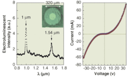
Recently, in collaboration with SVT Associates (Eden Prairie, MN), we have successfully synthesized and characterized Er:AlGaN/GaN QWs.9 Under UV pumping, the 1.55-µm emission from the QWs exhibited a marked improvement compared to the uncapped Er:GaN films. The enhanced emission appears because of more effective confinement of electron-hole pairs in the QW region, leading to a more efficient energy transfer from the electron-hole pairs to the Er ions. Based on these results, we have fabricated and demonstrated the operation of the first 1.55-µm current-injection LED based on p-AlGaN/GaN-Er/n-AlGaN QWs (see Fig. 4).9 Such structures form the basis for electrically pumped optical amplifiers.
Potential impact of InN
One of the interesting and important recent developments in nitride research is the determination of the energy gap of InN. Traditionally, a value of 1.89 eV at room temperature has been accepted. However, with improvement of material quality, recent data from many groups indicate a value of 0.7 to 0.8 eV.10, 11
Consequently, the band-edge transition of InN coincides with the communication wavelength. In addition, InN has unique material properties such as smallest effective mass, largest mobility, highest peak and saturation velocities, and smallest direct bandgap among nitrides. Due to the lack of high quality material, InN is also the least studied III-nitride.
The quality of currently available InN is still relatively poor because of the low dissociation temperature, high equilibrium vapor pressure of N molecules and the lack of suitable substrates. However, with its potential applications and worldwide effort, rapid progress is anticipated. Its true potential will be revealed with further improvement of epilayer quality and a better understanding of its material properties.
Overall, the III-nitride materials have occupied the center stage in the semiconductor R&D effort for the last decade with the main focus on photonic devices operating in the visible and UV regions. We believe that III-nitride photonics hold great promise for optical communications at 1.55 µm. Many fundamental issues must be addressed, however, before this goal can be realized. Specifically, further studies are needed on the optical-propagation loss, temperature sensitivity, polarization effects in InGaN/AlGaN heterostructures, carrier-induced change of the index of refraction, modulation efficiency, and modulation-induced polarization effects. Mechanisms that would enhance the
Er emission at 1.55 µm in Er-doped nitrides must also be explored. Novel designs for device integration must also be developed. As further improvements in material quality as well as fundamental understandings are achieved, it is conceivable that the future of III-nitrides for optical communications applications will be as bright as for blue/green and UV applications.
REFERENCES
- S. Nakamura et al., The Blue Laser Diode—The Complete Story (Springer, New York, 2000).
- R. Hui et al, Appl. Phys. Lett. 82, 1326 (2003).
- C. Gmachl et al., Appl. Phys. Lett. 77, 3722 (2000).
- N. Lizuka et al., Appl. Phys. Lett. 77, 648 (2000).
- K. Kishino et al., Appl. Phys. Lett. 81, 1234 (2002).
- H. X. Jiang et al., Appl. Phys. Lett., submitted.
- R. G. Wilson et al., Appl. Phys. Lett. 65, 992 (1994)
- J. E. Colon Mat. Res. Soc. Symp. Proc. 301, 169 (1993).
- J. M. Zavada et al., Appl. Phys. Lett., submitted & Mater. Sci. Eng. B, Elsevier, in press.
- T. Inushima et al., J. Cryst. Growth 227, 481 (2001).
- J. Wu et al., Appl. Phys. Lett. 80, 3967 (2002).
HONGXING JIANG and JINGYU LIN are professors of physics at Kansas State University, Manhattan, KS 66506-2601; e-mail: [email protected] and [email protected]. RONGQING HUI is an associate professor with the Department of Electrical Engineering and Computer Science at University of Kansas, Lawrence, KS 66045; e-mail: [email protected]. JOHN ZAVADA is a program manager in the Electronics Division at the U.S. Army Research Office, Research Triangle Park, NC 27709; e-mail: [email protected].


