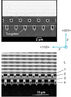
An experiment using a three-dimensional (3-D) tungsten photonic crystal may enable ultra-efficient light bulbs that can turn excess heat into light. Jim Fleming and Shawn Lin at Sandia National Laboratories (Albuquerque, NM) have reported promising measurements and simulations using a microscopic tungsten filament with an internal crystalline pattern. If applied to incandescent electric bulbs, the material could increase their efficiency from 5% to more than 60%.
The 3-D silicon photonic crystal was made by layering one-dimensional rods in a pattern that repeated every four layers (a unit cell). Fleming and Lin, along with researchers at Iowa State University (Ames, IA), then selectively removed silicon (Si) from existing polysilicon/silicon dioxide structures and back-filled the holes with tungsten in a chemical-vapor-deposition (CVD) process. Tungsten film does not adhere to silicon dioxide by CVD, so a blanket film was grown on a 50-nm-thick titanium nitrate adhesion layer that was deposited by reactive ion sputtering.
The complementary metal-oxide semiconductor fabrication technique is a variation on microelectromechanical-systems processes developed at Sandia's Microelectronics Laboratory. Because the work is performed on standard, commercially available 6-in. Si wafers, the tungsten photonic crystal is expected to be easily reproducible and inexpensive.
The group measured the optical properties of the sample across a wide range of infrared (IR) wavelengths from 1.5 to 25 μm. At 8 μm, the absolute reflectance of the tungsten photonic crystal increased while the transmittance showed a simultaneous decrease, indicating the presence of a photonic bandgap. Results of calculations for a four-layer 3-D crystal confirmed that near complete attenuation occurred from 8 to 20 μm—an unusually large bandgap—due to the photonic-bandgap effect. Measurements confirmed an impressive attenuation of 30 dB per unit cell at 12 μm. In the photonic-bandgap effect, suppressed IR energy is forced into a selective emission band at the edge of the photonic band, effectively funneling it into a more useful emission band.
According to Kirchoff's law, says the team, the absorbed (and thus lost) IR is equal to the emission rechanneled to other wavelengths. Although the work was done at mid-IR wavelengths, no practical difficulties are expected to prevent the shifting of this capability into visible wavelengths, which could lead to ultra-efficient light emission with a fraction of the energy lost to heat. The tungsten 3-D crystal was resistant to temperatures as high as 1500°C.
The results are also applicable to thermal photovoltaic (TPV) applications. Calculations show that the conversion of radiation to electricity in the tungsten crystal would improve the efficiency of a TPV application to 51% compared to 12.6% efficiency achieved in blackbody absorbers. The team reported that broad-background absorption of photons may be a practical limitation to achieving that efficiency.
REFERENCE
1. J. G. Fleming et al., Nature 417, 52 (May 2002).
About the Author
Valerie Coffey-Rosich
Contributing Editor
Valerie Coffey-Rosich is a freelance science and technology writer and editor and a contributing editor for Laser Focus World; she previously served as an Associate Technical Editor (2000-2003) and a Senior Technical Editor (2007-2008) for Laser Focus World.
Valerie holds a BS in physics from the University of Nevada, Reno, and an MA in astronomy from Boston University. She specializes in editing and writing about optics, photonics, astronomy, and physics in academic, reference, and business-to-business publications. In addition to Laser Focus World, her work has appeared online and in print for clients such as the American Institute of Physics, American Heritage Dictionary, BioPhotonics, Encyclopedia Britannica, EuroPhotonics, the Optical Society of America, Photonics Focus, Photonics Spectra, Sky & Telescope, and many others. She is based in Palm Springs, California.
