Newsbreaks
The mechanism involved in the green upconversion consists of two consecutive energy transfers from the Yb to the Ho. Upon short-pulse excitation, the green emission decays over a time span of approximately 0.2 ms. Upon continuous-wave excitation, the red emission rises relatively slowly over a period of milliseconds. Contact Witold Ryba-Romanowski at [email protected].
Intracavity Dove prism boosts OPO beam qualityOptical parametric oscillators (OPOs) pumped with nanosecond pulses typically have poor beam quality as a result of the required short cavities and large beam diameters. Researchers at Sandia National Laboratories (Albuquerque, NM) are reducing this problem by inserting a beam-rotating Dove prism into the cavity. The OPO contains a 15-mm-long potassium titanyl phosphate crystal cut for collinear phase matching of 532-nm light to 800-nm plus 1588-nm light, and placed in a ring recirculating cavity with a triangular path.A Brewster-angled Dove prism is inserted at 45° to the plane of the ring; the three mirrors invert the beam in one direction each pass through the cavity, while the Dove prism inverts the beam about a plane parallel to its base. The combination results in a 90° beam rotation for each pass. A beam displaced from the axis overlaps itself every fourth pass. Before insertion of the prism, the beam is elliptical, while after insertion it assumes an almost perfect circular Gaussian shape surrounded by a small shoulder. Contact Darrell Armstrong at [email protected].
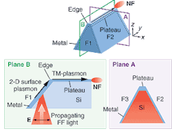
Plasmon waveguide converts far-field to near-field lightAs optical integrated circuits grow in complexity, their features must shrink in dimension to limit overall circuit size. Researchers at the Tokyo Institute of Technology (Yokohama, Japan) and the Japan Science and Technology Corp. (Tokyo, Japan) have developed a technique for converting far-field light to near-field light (having a beam width of subwavelength dimensions) and channeling the near-field light. If put into practice, the technique may enable the use of the optical nearfield as a carrier for signal transmission over distances of a few microns within a circuit.The technique makes use of a plasmon waveguide running along the edge of a gold-plated silicon wedge. The edge is actually a plateau of 150-nm width and 80-μm length. The wedge itself is kept to a height of 10 μm to keep transmission loss low at the 830-nm experimental wavelength. Far-field light entering the wedge is converted to a two-dimensional plasmon mode on the wedge's surface and then to a one-dimensional plasmon mode on the plateau. A 150-nm-wide mode was transmitted over a distance of 2.5 μm; narrower plateaus should enable modes 100 nm wide or smaller. Contact Takashi Yatsui at [email protected].
All-Raman-amplified spans transmit at 10 petabit-km/s In the field of fiberoptic communications, so-called hero experiments do have their place. Though it is sometimes difficult to sort through the various combinations of transmission length and data rate, multiplying data rate by distance gives a single number that can be used for the purpose of claiming records. A solid front-runner in this respect is Lucent Technologies (Holmdel, NJ and Murray Hill, NJ), where a group of researchers has transmitted 2.5 Tbit/s (64 x 42.7 Gbit/s) over 4000 km of non-zero-dispersion-shifted fiber, for a record of 10 petabit-km/s.In the setup, 64 distributed-feedback lasers operated on a 100-GHz ITU grid, ranging from 1554.6 to 1607.0 nm; two 32-laser transmitters on a 200-GHz grid were interleaved in an arrayed-waveguide grating router. Two external lithium niobate modulators were driven in a push-pull configuration to minimize chirp. A 10.664-Gbit/s pseudorandom bit stream was electrically multiplexed four times with time delays to provide the data for each channel. A recirculating loop consisted of five 100-km spans of reduced-slope fiber, Raman amplifiers, and dispersion-compensating fiber modules. The result was a corrected bit-error rate of less than 1 x 10-12. Contact Alan Gnauck at [email protected].
Optically pumped lead-salt VCSEL operates at 320 KMid-infrared lasers with wavelengths that match the absorption spectra of gases are valuable for atmospheric monitoring. Electrically pumped edge-emitting lead-salt diode lasers cover these wavelengths, but cannot achieve room-temperature operation in continuous-wave (cw) mode because of low thermal conductivity. Researchers at the University of Oklahoma (Norman, OK) have developed an optically pumped lead-salt vertical-cavity surface-emitting laser (VCSEL) that operates in pulsed mode at up to 320 K and has potential for room-temperature cw operation.Based on a lead selenide/lead strontium selenide quantum-well structure, the VCSEL is pumped by a 1.06-μm-emitting Nd:YAG laser, with the intent being to pump it with a 1-μm-emitting laser diode. The VCSEL emits a maximum power of 40 mW at a 4.12-μm wavelength. A low-quality top mirror broadened the spectral emission width to 50 nm. Improving the top mirror and adding a pillar to the cavity should reduce the linewidth and may allow cw operation. The laser could be made tunable with the addition of an adjustable top mirror or external-cavity tuning. Contact Zhisheng Shi at [email protected].
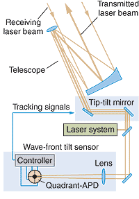
Quadrant-APD-equipped laser tracker compensates to 1 μradA group at the Communications Research Laboratory (Tokyo, Japan) is studying the effectiveness of silicon quadrant-type avalanche photodiodes (APDs) for use in laser tracking systems. As in non-APD quadrant detectors, the device under test, made by Hamamatsu Photonics (Hamakita-City, Japan), measures the two-dimensional position of a laser spot impinging on it. The APD quadrant detector has a diameter of 1.5 mm and a deadband width (width of the nonactive stripe between quadrants) of 35 μm. Its quantum efficiency is 80% at a wavelength of 800 nm, while its -3-dB bandwidth is 2.3 kHz, limited by the feedback resistor. The detector's multiplication factor reaches 30 before saturation occurs in one of its quadrants.The researchers built a laser tracking system intended for compensating the angular error of a transmitted laser beam for a free-space communications link. The APD monitored the tilt of an incoming laser wavefront (see figure). The noise-equivalent angle of the system was several times better than for a conventional quadrant detector, reaching 1 μrad for a received optical power of 4 pW. Contact Masahiro Toyoda at [email protected].
Far-infrared quantum detector bests bolometersA far-infrared (FIR) optical detector developed by a group at the University of Tokyo (Tokyo, Japan) exploits the cyclotron resonance of two-dimensional electrons in doped aluminum gallium arsenide/gallium arsenide heterojunctions. Fabricated in a configuration called a Hall bar and operated at 4.2 K, the device has a responsivity of 1.1 x 10⁷ V/W, a figure 1000 times larger than commercially available bolometers. The device's detectivity reaches 4 x 1013 cm · Hz½/W at its peak spectral performance, or an order of magnitude higher than commercial bolometers.The detector has a geometry with a 167-mm length and a 50-μm width fitted in a snakelike fashion within a 4 x 4-mm region. Radiation causes a change in resistivity of the detector; sensitivity peaks at 180 μm. The group characterized the device with a broadband FIR source containing a metal film heater deposited on a thin sapphire plate as a calibration source. To wring every last bit of performance from the detector, the researchers lowered its temperature to 1.5 K, boosting its responsivity to 2 x 10⁷ V/W. Contact Yasushi Kawaguchi at [email protected].
Chalcogenide glass is highly nonlinear at 1.55 μmGlasses with high optical nonlinearities have potential applications in ultrafast all-optical switches (AOSs), in which a phase shift induced in a waveguide Mach-Zehnder interferometer by a change in intensity causes switching. For a nonlinear glass to function well in an AOS, its figure of merit (FOM; a dimensionless number relating nonlinearity to nonlinear absorption) should be greater than 5. Researchers at Cornell University (Ithaca, NY) and the Naval Research Laboratory (Washington, DC) have fabricated several types of chalcogenide glass based on arsenic, sulfur, and selenium, with some having a FOM of 5 or greater at wavelengths of 1.25 or 1.55 μm and Kerr nonlinearities 400 times or more than that of fused silica.In the glass samples of highest interest, a nonlinear phase shift of π rad is produced at intensities of less than 200 MW/cm2, a level that causes no damage to the glass. The researchers determined that the high optical nonlinearity is caused mostly by the presence of selenium, and identified one glass as particularly well-suited for use at 1.55 μm. Contact Jeff Harbold at [email protected].
Experiment and theory agree for self-written waveguidesResearchers at Osaka University (Osaka, Japan) and Australian National University (Canberra, Australia) have constructed self-written waveguides in a photopolymer and have developed an analytical model of their creation, thereby aiding the study of their properties. This method of waveguide production could be useful in the fabrication of X and Y junctions used in photonic devices for telecommunications.Soliton-induced waveguides can be "frozen" in a photopolymer, but the question is whether the waveguides preserve the properties of the initial solitons. The researchers start with a polymer in which waveguides can be self-written via a single-photon process. A helium cadmium laser writes two waveguides whose axes collide with each other; the structure is imaged by a charge-coupled-device camera. Two 0.1-mW beams colliding at a 6.4° angle write separate waveguides that merge into one. Beams of unequal power create waveguides tilting in a different direction than that resulting from the merging of solitons alone. Stationary analytical solutions worked out by the researchers coincide with the experimental results. Contact Satoru Shoji at [email protected].


