Edge-emitting III-V LEDs illuminate wearable color microdisplays
BY ERIC ALTENDORF
Scanned microdisplays offer several advantages over active-matrix displays such as thin-film transistor liquid-crystal displays (TFT-LCDs) and liquid-crystal on silicon (LCOS). Three RGB light sources and a scanning mirror are the principal components of a scanned microdisplay, or retinal-scanned display (RSD). In principle, such a system can be produced inexpensively, with a compact form factor suitable for cell phones and wearable applications. Directly modulated, high-brightness, diffraction-limited sources are required, however, for optimal display resolution and brightness. Single spatial-mode laser diodes are ideal light-source candidates, but currently only red commercial devices and blue (≥450 nm) engineering samples are available. Thus III-nitride edge-emitting light-emitting diodes (EELEDs) are being considered as alternative blue- and green-output light sources for scanned microdisplays, and prototype EELED-based RSD microdisplays are under development at Microvision Inc. (see "How does a scanned microdisplay work?" on p. 56).
Red visible (635 nm ≤ λ ≤ 665 nm) single-mode laser diodes based on aluminum gallium arsenide (AlGaAs) and aluminum indium gallium phosphide (AlInGaP) material systems are commercially available. In 1995, Shuji Nakamura and coworkers at Nichia Chemical Industries (Tokushima, Japan) succeeded in producing the first violet-emitting laser diode based on the III-nitride material system, named so because all of the elements except for nitrogen are found in the third column of the periodic table.1
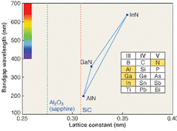
Indium gallium nitride/gallium nitride (InGaN/GaN) is used for the active regions of III-nitride LEDs and laser diodes, producing emission wavelengths that can be tuned over most of the visible spectrum by varying the concentration of indium. Bright blue and green III-nitride LEDs that vastly outperform earlier GaP- and silicon carbide (SiC)-based LEDs are now available from a variety of device manufacturers. A significant lattice mismatch exists, however, between the commonly used SiC or sapphire substrates, and the epitaxial AlInGaN over-layers that make up III-nitride devices (see Fig. 1). As a result, threading dislocation-defect densities as high as 1010/cm2 are common in III-nitride epitaxial materials.

FIGURE 1. Wavelengths correspond to the bandgap energy vs. lattice constants for three binary alloys in the III-nitride material system. Dotted and dashed lines indicate lattice constants for two common substrates. The emission wavelength for III-nitride LEDs and laser diodes is determined by the indium concentration in the GaN/InN active region. Higher In active regions produce longer-wavelength devices. Significant differences in lattice constants result in high defect concentrations, as well as strain in III-nitride devices.
Interestingly, the high defect densities do not significantly impact LED performance. Only at the higher current densities required for laser diodes do the defects become a limiting factor. Defect-density reduction using novel epitaxial-growth techniques have pushed III-nitride cw laser-diode wavelengths out to 450 nm and beyond. Unfortunately, the difficulty in producing efficient high-current-density devices increases dramatically as the indium concentration and emission wavelength increases, and it is not clear when a viable green III-nitride cw laser diode will be available.
Edge-emitting LEDs
An alternative to using laser diodes is to use EELEDs.2, 3 The EELED structure is similar to a ridge-waveguide laser diode (see Fig. 2). Current is injected along a narrow stripe producing light that is guided to the end of the ridge, where it exits through a laser-diode-like facet. The current densities are similar to that of a laser diode (~kA/cm2), and as a result the efficiencies of III-nitride EELEDs are low. Specifically, the gain in these devices is insignificant, meaning that the optical power and drive-current relationship and spectral distribution correspond to an LED, not a laser diode.
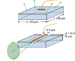
The usable RSD microdisplay optical-power levels (power collected by a collection numerical aperture of 0.1) are at most several microwatts, compared to milliwatts for laser diodes. However, the small emission area (<10 μm2) and relatively narrow far-fields of these EELEDs result in brightness levels one to two orders of magnitude higher than comparable surface-emitting LEDs. For example, a surface-emitting LED with an area of 100 x 100 μm delivering 5 mW of total optical power would put less than 0.05 μW into an emission aperture of 0.1 NA from an area equivalent to an EELED.
The laser-diode-like structure also means that EELEDs have response times of a few ns, adequate for scanned-display applications. The high internal quantum efficiency of the materials used for red EELEDs implies that lasing needs to be suppressed by modifying the facets or limiting the length of the current injection stripe. An advantage to using EELEDs is that the optical power vs. current dependence is nearly linear, allowing for simpler drive electronics than laser diodes. Edge-emitting LED operation is also less dependent on ambient temperature changes, and image artifacts due to laser speckle are absent.
Full-color prototypes
Microvision has produced several full-color microdisplay demonstrators that use custom blue and green III-nitride EELEDs produced by Cree Research Inc. (Durham NC) and red AlInGaP EELEDs supplied by Advanced Chips and Products (AC&P; Hillside, NJ). Several VGA (640 x 480 pixels) RSD microdisplays and SVGA (600 x 800 pixels) full-color demonstrators have been produced. Efforts are under way to improve the collection efficiency of the RSD microdisplay optics and the intrinsic brightness of the EELEDs.
The principle limitation is the availability of green EELEDs at wavelengths above 520 nm with adequate optical-power levels. For systems with optimal green devices, the range of available display colors can exceed CRT and LCD standards (see Fig. 3). Whether laser diodes or EELEDs, III-nitride blue and green high-brightness sources are critical components in the development of this technology toward high-resolution, compact, and potentially low-cost microdisplays.
REFERENCES
1. S. Nakamura and G. Fasol, The Blue Laser Diode (Springer; Berlin, 1997).
2. D. C. Bertolet et al., Proc. SPIE 3621, 249 (1999).
3. E. Altendorf et al., Proc. SPIE 4445, 111 (2001).
ERIC ALTENDORF is a senior staff engineer at Microvision Inc., 19910 North Creek Parkway, Bothell, WA 98011; e-mail: [email protected].
How does a scanned microdisplay work?
The essential components of a scanned microdisplay system are diagrammed in Fig. S1. For simplicity only a single source is considered, and only a single scan direction is indicated. A full two-dimensional display would also scan in the direction orthogonal to that shown in Fig. S1, either by using a second mirror or a single biaxially scanned mirror. Combining red, green, and blue sources prior to the collection lens produces a full-color display. A screen placed at the intermediate image plane allows direct viewing of the scanned image, or an ocular can be employed to relay the scanned beam into the eye. In the latter case, the system scans the image directly onto the retina, and is referred to as a retinal-scanned display or RSD.1 These different configurations do not alter the following conclusions.
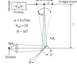
The principal components are a visible source, a collection optic, and a scan mirror. The maximum optical scan angle is equal to twice the maximum mirror rotation angle (θopt = 2θ). For example, a mirror positioned at 45° to the incident beam deflects the beam by 90°. The scan mirror also determines the maximum limiting aperture, NA|, prior to the image plane. The smallest scanned spot, and hence the highest resolution, is determined by the diffractive point-spread function of the converging beam. In this case, the focused spot at the image plane is said to be diffraction-limited.
The size of the focused spot at the image plane is given by ω = kλ/NA|, where NA| is the numerical aperture, defined as the sine of the half-angle of the converging cone of light; λ is the wavelength, assuming a spectrally narrow light source; and ω is the full width at half-maximum (FWHM) of the focused optical-intensity distribution. The constant k incorporates details of the beam-intensity profile and mirror-shape factors. Typical NA| and θopt values are small, such that NA| is proportional to D/2f, and the total linear scan displacement is given by L = fθopt. Combining these relationships gives N = βθD, where N is the maximum number of resolvable pixels (N = L/ω), and β is a constant that depends on the nominal scan-mirror angle relative to the optical feed beam (shown as 45°), as well as beam-intensity profile and mirror-shape factors. It follows that the display resolution is fundamentally limited by the θD parameter of the scan mirror.

The best display resolution for a given θD is realized when the size of the scanned spot is diffraction-limited. In this case, propagating the beam back through the system suggests that the ideal source is itself diffraction-limited. This implies that the emission NA of the source, NAs, is matched to the collection numerical aperture of the system, NAc. Single spatial-mode laser diodes and optical fibers are good candidates for such light sources. Microvision RSD microdisplays typically have a collection numerical aperture, NAc, of about 0.1, which corresponds to a half-angle of 5.74°. Light sources that emit into such a numerical aperture have spatial dimensions of at most a few microns, a characteristic of laser diodes. Larger-area sources such as conventional surface-emitting LEDs exhibit broad far-field emission angles and need to be masked to limit the emission area to laser-diode-like dimensions. Both properties drastically reduce the available power for RSD microdisplay applications.
Light-source brightness or luminance, is defined by the photometric power (Lumens) emitted per solid angle, per area, of the source (see Fig. S2). For conventional projection systems, display brightness is related to the source brightness through the equation Bdisplay = Bsource.t.
The factor t incorporates the reduction in brightness caused by optical transmission losses and scattering. In scanned displays, an additional factor is needed to account for the limited pixel duty cycle: Bdisplay = Bsource.t.dc.
Rearranging this equation gives Bsource = (Bdisplay/t).(1/dc). For an SVGA display with 600 x 800 pixels, 1/dc is greater than 480,000, demonstrating that the source brightness needs to be significantly greater than the display brightness for scanned display systems. Adequate capability for direct modulation is a further requirement for scanned microdisplay sources. For a scanned SVGA display with a screen refresh rate of 60 Hz, the time interval corresponding to a single pixel is about 20 ns. Standard surface-emitting LEDs have response times equal to or greater than 20 ns, implying that these sources do not respond rapidly enough for scanned microdisplay applications.
REFERENCE
1. Microvision Inc. web page: www.mvis.com.