Researchers from Heriot-Watt University (Edinburgh, Scotland) and Shlumberger Test and Transactions (San Jose, CA) have collaborated to demonstrate a new way of imaging buried active integrated circuits. Based on the two-photon optical-beam-induced current (TOBIC) effect, it allows 1-µm or better resolution in all three dimensions. The technique is particularly appropriate for chip testing because it generates a current relative to the output pin used in each imaging cycle. As a result, it can provide an interconnectivity map that can be vital to understanding chip operation. Researchers are now looking at ways of comparing the TOBIC results with original design schematics.
Getting a clear picture of the structure of a microelectronic chip is difficult—the most interesting and relevant information is often hidden by metallization layers. In the case of flip-chip-bonded devices common in optoelectronics, the two active areas are sandwiched between chip substrates. The TOBIC effect is one of several phenomena that can be exploited to overcome this problem. It is caused by the fact that, when they receive sufficient energy, electrons can be released from their initial position and allowed to move. Such movement can occur by simply using photons of sufficiently high energy. By using two photons, however, the selectivity of the process can be greatly increased, because the current is only generated in the volume where the light intensity is sufficiently high to allow pairs of photons to be absorbed simultaneously. Though this makes it inefficient compared to one-photon techniques, it also significantly improves image resolution.
The researchers use a modelocked femtosecond 1.275-µm-emitting optical parametric oscillator as their two-photon source.1 The device has a repetition rate of 110 MHz, an average excitation power of 50 mW, and a full-width half-maximum pulse duration of 160 fs. The beam is directed through a simple two-lens telescope after being scanned in two dimensions by orthogonal galvanometric mirrors, and then propagates through a microscope setup with a 50×-magnification objective.
A piezoelectric actuator attached to the translation stage is used to move the chip under inspection up and down through the microscope's focal plane. This allows confocal sectioning. Before being examined, the chip in question must have its substrate thinned significantly: this prevents one-photon absorption—which can swamp the TOBIC effect in thick semiconductor samples—from becoming a problem.
Seeing current
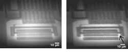
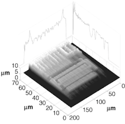
The contrast in the resulting images is a function of both the material and chip wiring (see Fig. 1). Light areas show large currents, which means that the area is both conductive and the current created is reaching the pin attached to the detector. Dark areas either depict areas that are highly insulating or those that are not connected to the relevant pin. This results in a certain amount of ambiguity, because the precise meaning of the different shades of gray cannot be calibrated in a single shot. Nevertheless, by combining data from the areas with the same current readings, pictures of three-dimensional structures have been successfully produced (see Fig. 2).Work by the researchers continues on trying to exploit the pin dependence of the TOBIC process. According to Derryck Reid, head of the Ultrafast Optics Group in the Heriot-Watt Physics Department, they are currently working on exploiting multipin data. This can be used both to minimize ambiguity as to the conductivity of the sample and to examine how the device is wired up. By combining this data with the chip designers' plans, this passive technique should be able to provide valuable information about chip-implementation problems before active electronic testing begins.
Another projected improvement is to use low-noise acquisition of the TOBIC signals. This should suppress noisy spikes that currently occur when no heavily-doped or metallized features are present—spikes caused by the fact that signals from outside the volume of interest can significantly effect the desired signal if it is very small. With this advance, researchers say it might be possible to detect and image the interfaces between epilayers in structures such as light-emitting diodes and vertical-cavity surface-emitting lasers.
REFERENCE
- E. Ramsay et al., Appl. Phys. Lett. 81(1), 7 (July 1, 2002).
About the Author
Sunny Bains
Contributing Editor
Sunny Bains is a contributing editor for Laser Focus World and a technical journalist based in London, England.

