Lithography aids integration of optics
Norman Hairston
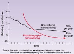
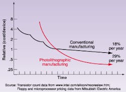
Lithographic production permits the integration of multiple functions within a planar optical structure and the simultaneous production of multiple copies of devices.Planar lithographic production of optical components used in fiberoptic communications presents a superior means to lower costs compared to conventional cost-reduction methods. Migration to a low-wage manufacturing site, materials substitution, and training, for example, have limited ability to cut costs. The use of planar lithographic integration, on the other hand, continually increases the number of devices that can be made from a given amount of labor, capital, and material, and reduces the number of individual components while increasing functionalityjust as it did in the semiconductor industry (see Fig. 1).
Although lithographic fabrication of optical devices requires different materials from those used in electronics, the processes are the same and the knowledge from 40 years of semiconductor production is applicable. Particularly important is the fact that required lithography equipment is already widely available, as are experienced operators and designers.
Traditionally in fiberoptic communications, the function of optical components was primarily passivecomponents served merely as conduits or passive steering elements for the optical signal. Fulfillment of these functions was easily accomplished with bulk optics made by conventional means from conventional materials such as fiber, filters, lenses, evanescent couplers, splitters, and taps. Widespread implementation of dense wavelength-division multiplexing into optical networks has brought more-exotic processes and materials into optical-component manufacture.
Silica on silicon (SOS) was among the first planar technologies to be applied to the manufacturer of optical components. Devices such as arrayed waveguides are built from SOS technology using photolithographic deposition techniques. Though these devices have contributed to the enormous increases in the capacity of existing optical networks, and though they employ photolithography in their manufacture, the devices produced still use conventional materials systems and still are limited to passive (not actively controllable) steering of the optical signal.
Going for transparency
The greatest challenge in the development of end-to-end, higher-speed, higher-capacity networks is in eliminating the optical-to-electrical-to-optical (OEO) conversions that slow transmission and add protocol restraints. These transitions are necessary to groom and redirect the optical signal onto and off of the high-speed optical portion of the network. They are particularly necessary in the metro and local portions of the network where the signal is close to its origin or destination. Each OEO conversion involves receiving, decoding, processing, redirecting, and relaunching the optical signal. Even with the fastest electronics operating at the speed of light, this process takes a tremendous amount of time and results in a significant increase in the end-to-end travel time of the signal and a reduction in network capacity. The entire OEO process is analogous to changing planes at a busy airport on a cross-country trip; the signal spends a significant proportion of its transition time sitting at a hub.
The all-opticalor transparentportion of the network is OEO free and protocol independent. Increasing the transparency of the network enables both higher speed and higher data-carrying capacity from already installed assets. Carriers, faced with declining prices and increasing demands for higher speed and more flexible services, must find ways to cut costs. Increasing transparency is the answer.
Carriers trying to build profitable transparent networks and bring increased and burstable capacity closer to users through metro mesh networks face two considerable barriers. First, optical devices need to take over control functions that are being done electronicallyspecifically, amplification, attenuation, and switching. Second, the devices need to be made cheaply enough, and in large enough volume, so they can be employed in the higher-density meshes of the metro and local levels of the network. Lithographic manufacturing meets both of these requirements; indeed lithographic production may be the only option for network providers to quickly meet pressing equipment cost objectives.
The promise of planar lithographic integration is for an immediate reduction in labor, packaging, and testing costs; then, with subsequently higher levels of integration, reducing these costs further. Lithographic production innovations also promise to improve device performance by reducing the number of optical interconnections with their resulting insertion losses.
Optics vs. electronics
Lithography quickly replicates a prototype from chip to chip, wafer to wafer, or substrate to substrate. A lithographic system for producing optical components uses virtually the same set of tools as with electronicsthe exposure tools, masks, resists, and all of the processing steps to accomplish a pattern transfer from mask to resist and then to device. However, there are significant differences.
Starting with the circuit design procedures, there are two major differences in path layout between lithographically produced electronics and photonics. First, while bends and interconnects impact both the power levels and maximum data rates of both electronic and optical circuits, the great majority of the impact of an electronic path redirection is on the data rate, while the greatest impact of an optical path redirection is on the optical power throughput. A prime example is a severe bend.
While a severe bend is easily accomplished in an electronic circuit with minimal loss of electrical power, such a bend results in a virtual total loss of optical power in an optical circuit. Conversely, a bend can bring about a significant decrease in the maximum data rate for an electronic circuit, while the data rate of an optical circuit is largely unaffected by a bend.
The second circuit design consideration is that while electrons are interacting with each other, photons largely are not. Photons in the same plane can cross each other or even exist in the same conduit without interacting. As a result, much may be accomplished in an optical circuit within a single plane of activity. The result of both this consideration and the previous property is that while electronic integrated circuits tend to have an overall square geometry (to pack more into a single chip) with multiple layers to enable the crossover of electrical signals, integrated optical chips will tend to have a single layer and a long geometry with unidirectional flow to minimize bending of the optical path.
A second major difference between lithographically produced optics and electronics is the materials used. Electronics benefit from the use of silicon, which can be doped with various other materials to produce a wide variety of electronic functions. No optical analog of silicon exists. Different functions in optics, such as routing, amplification, or attenuation, tend to be carried out by completely different materials. Coupled with the circuit design considerations, the result is a kind of "serial integration" for lithographically produced optical devices that integrate multiple functions. One optical chip in one material performing one set of functions must be coupled with a subsequent chip of a different material performing subsequent functions. The resulting assembly tends to have more function resemblance to an electronic circuit board that a monolithic silicon chip, with a heterogeneous materials set employed. Important lithographically processable optical materials include lithium niobate (often used as a high speed electro-optic modulator material), gallium arsenide, indium phosphide (used as laser, amplifier and modulator), and silica (splitting, routing, spectral filtering, andif dopedamplification). Polymer waveguide systems are a new and exciting materials class for switching, attenuation, modulation, or routing applications needing high performance at lower cost.
A third significant design difference between lithographically produced optics and electronics is the component packaging. While many of the functions of an electronic and optical package are similar (environmental protection, heat conduction, electromagnetic isolation), the paradigm difference between a hybrid circuit board vs. a monolithic silicon chip dictates that integrated optical fabrication involve not only lithography, but attach and alignment tasks. In addition to everything else, the packaging must secure the heterogenous materials to each other without the possibility of detrimental interactions, must accommodate differing rates of thermal expansion, and must maintain alignment of the optical elements.
With conventional bulk optics, alignment involves locating a succeeding optical element within five degrees of freedomcentered in X, Y, and Z space and oriented with a minimum of pitch and yaw. With lithographically produced optical elements, the chips tend to be arrays of optical pathways. Therefore, a sixth degree of freedomrollis added to the difficulty. So, attachment and alignment of integrated optical devices is not only more complex than electronics, it requires a higher degree of precision than even conventional optics.
Cost-reduction mechanisms
Two principal mechanisms enable planar lithographic production to bring about cost reduction for optical devices; both involve incorporation of multiple elements into a single integrated manufacturing process. The first is the functional aggregation of serial integration; the second is array or parallel scaling.
Serial integration is the implementation of multiple optical functions into a single device. As much as 80% of the cost of an optical device is in the optical interconnection and packaging. By incorporating multiple functions into a single device, packaging costs are saved along with an overall reduction in the aggregate size of the devices and of the equipment in which they are ultimately used.
Serial integration also results in a net performance improvement. Most optical systems tend to be optical-power limited. With conventional optics, there is a significant loss of optical power between each element. By enabling a net reduction of the number of elements in an optical pathway, serial integration conserves optical power and reduces the need for additional amplifiers to compensate for previous lossy interconnects.
The second principal cost-reduction mechanism of planar lithographic manufacturing is array or parallel scaling, in which multiple copies of the same device are manufactured simultaneously. As with serial integration, each copy also saves an additional optical package, with its associated costs. While some of the benefits of serial integration may be accomplished through use of a common package for a series of bulk optical elements, the benefits of parallel scaling may only be attainable through the use of lithographic production methods.
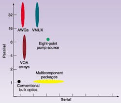
The full benefits of optical integration come from using both serial and parallel integration (see Fig. 2). Applying lithographic production technology to the integration of multiple optical elements and functions on a single planar device results in a fundamental shift in the way fiberoptic components are manufactured. Tedious manual fabrication with low yields is eliminated.
Implementation
One example of combining both serial and parallel integration benefits is a multiport pump source developed by Gemfire. Designed to take full advantage of lithographic production, a high degree of device integration yields eight independently controllable fiber outputs from a compact optical module that includes integrated laser frequency stabilization and front facet power-level sensing.
Normal production of semiconductor lasers produces arrays of lasers that are subsequently diced, electrically and optically connectorized, and individually packaged to produce individual pump lasers. The integrated pump source uses a laser array that is not diced. The array is electrically connectorized and coupled to an optical chip that provides laser stabilization, mode matching between the lasers and output fibers, and output power sensing. The resulting multiport device goes into a single hermetic package. The single package for eight lasers eliminates the need for seven thermoelectric coolers, reducing electronic component costs as well as optical component costs.
NORMAN HAIRSTON is marketing manager at Gemfire Corp., 2471 East Bayshore Road, Suite 600, Palo Alto, CA 94303; e-mail: [email protected].