Semiconductor manufacturing techniques for ferroelectric liquid crystal microdisplays
MARK HANDSCHY
Microdisplays open up lucrative new market opportunities for semiconductor chips by directly adding display functionality to integrated circuits. Microdisplays serve as viewfinder displays for camcorders and digital still cameras, and they are used in the projection engines of projection televisions and computer monitors. The users of these consumer products see an image of the surface of the microdisplay chip that is enlarged by viewing or projection optics, making the apparent size of the display much larger than that of the chip supplying the image.
The advent of microdisplay products is motivated by straightforward market and technology dynamics. Through the capabilities of ever-advancing CMOS technology, microdisplay pixel size can be shrunk so that increased resolution can be delivered essentially free of charge. In addition, the small form factor and low power consumption of microdisplays are desirable for portable and mobile products. The microdisplay's ability to deliver high resolution without compromising portability will make possible new classes of information "appliances," such as wearable computers and wireless internet terminals. Finally, the reliance on intermediate optics to enlarge the image of the microdisplay allows the apparent display diagonal size to be scaled up without corresponding increases in display system cost.
Microdisplay options
Several approaches are being pursued for the delivery of these die-scale displays. At present, the microdisplays with the greatest market penetration are Texas Instruments' Digital Light Processing (DLP) products, which have found widespread use in business data projectors. The DLP products are based on TI's Digital Micromirror Device (DMD), a MEMS technology.1 A number of companies, including Displaytech, are developing liquid crystal on silicon (LCOS) products. These microdisplays are finding additional applications as viewfinders for electronic cameras and camcorders, and as projection elements for rear-projection HDTVs. Kopin is taking a unique LCOS lift-off approach that enables its displays to be transmissive, in contrast to the reflective nature of the other LCOS displays and the DMD displays. The last microdisplay approach is to add light-producing phosphors to the chip surface to make an emissive microdisplay, an approach being taken by a few other companies.
LCOS display structure
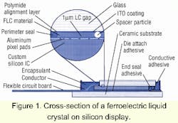
Figure 1 shows the construction of an LCOS microdisplay typical of the type being manufactured by Displaytech. This display shares with other LCOS displays the virtue of being built on foundry-supplied silicon, enabling the microdisplay manufacturer to use a "fabless" business model for silicon procurement. The additional liquid crystal (LC) processing steps also rely heavily on standard semiconductor and flat panel display (FPD) manufacturing processes, allowing the microdisplay maker to implement a manufacturing line with equipment from established makers that can be procured with minimal leadtime.
There are several types of liquid crystal materials that can be used in LCOS displays, including the proprietary ferroelectric liquid crystal (FLC) technology used in our displays. A typical FLC molecule is shown in Fig. 2. In the liquid crystal, these molecules line up with their long axes more or less parallel to each other, making an optically anisotropic phase that can rotate the polarization of light passing through. Changing the voltage applied to the liquid crystal changes the molecular-axis direction, which in turn switches the optical effect. The polar characteristic unique to FLCs lets the switching voltage actively drive them ON as well as OFF, eliminating the slow relaxation to OFF found in other LC types. The faster switching of the FLC makes possible single-panel, sequential-color products. The FLC speed is accomplished with drive voltages low enough to allow FLC microdisplays to be built on backplanes made in advanced low-voltage CMOS processes. These deliver the lowest possible power consumption while providing the greatest system-on-a-chip integration capability. Furthermore, the FLC cell gap, which is thinner than that of most other LCOS devices, permits the realization of the finest pixel pitches. Switching between optical ON and OFF states rotates the FLC optic axis in the plane of the electrodes, giving better contrast in fast (low f/#) optical systems than the out-of-plane rotation of other LCOS devices.
Manufacturing issues
LC microdisplay companies have universally adopted a fabless model where the starting CMOS wafers are purchased from a silicon foundry. The microdisplay maker then adds the LC functionality in a fab of its own or by using the LC device assembly services of a third party. In any case, the cost of the CMOS wafer is the dominant component of the total microdisplay bill of materials and is the major factor driving LC process choices. Assuming fixed pixel-array size and overall display-die electrical yield, the silicon-based cost of microdisplays can be reduced in two ways. First, the non-pixel die area can be reduced to increase the number of displays/wafer. Second, the yield of the LC post-processing steps can be increased to reduce the expensive fallout of the starting CMOS chips. The first factor is especially important for the smaller microdisplays used in viewfinders, for example, while the second factor is more important for the larger projection microdisplays.
Starting materials
The LC manufacturing line processes foundry-supplied CMOS silicon wafers along with specially coated glass wafers. The silicon wafers are obtained after being manufactured in a largely standard way. The main difference is enhanced last-metal reflectivity, which is typically obtained with thin (2000-3000Å thick) aluminum that is never exposed to high processing temperatures (<450°C). Cross-die planarity, which is essential to LC cell gap control, is optimized by careful placement of dummy geometry in the design layers, and by careful control of the chemical-mechanical planarization process. The wafers may be delivered to the start of the microdisplay line with little or no passivation oxide, dictating careful handling that avoids contact with the wafer face in order to prevent cosmetic blemishes.
For uniformity of handling, the glass wafers arrive at the start of the line as rounds the same size as the silicon wafers, typically 200mm, although squares provide a lower-cost alternative. An indium tin oxide (ITO) coating provides a transparent electrode that will form the common counter electrode for driving the LC. No patterning of the ITO is necessary, as all pixel definition is accomplished on the silicon backplane.
Wafer cleaning
After procurement of the starting glass and silicon wafers, the processing begins with cleaning of the substrates. The initial cleaning step serves to remove particles as well as organic films. Particle removal can be accomplished by washing in aqueous detergent or in solvent. Cleaning can be enhanced by megasonics or by scrubbing with a soft (e.g., polyvinyl alcohol) brush. These process steps must be carried out without reducing the reflectivity of the wafer surface or causing any cosmetic blemishes. Aqueous detergent chemistry must be adjusted to prevent corrosion if the last metal is unpassivated. A washed wafer must be dried before subsequent processing. This can be done by spin/rinse drying or by Marangoni drying, where the wafer is pulled through a meniscus into an atmosphere with IPA vapor.
Complete removal of organic contaminants, in-cluding residual detergents and surfactants, is important because variations in the surface wettability can adversely affect the quality of the following alignment layer. Additionally, organic contaminants soluble in the LC material will increase its electrical conductivity, which is undesirable. Organic films can best be removed by plasma cleaning or by exposure of the wafers to ozone generated by ultraviolet (UV) irradiation in an oxygen atmosphere.
Alignment
In almost all LC devices, the LC optic axis needs to be uniformly aligned throughout the device for it to deliver the desired optical performance. This is usually accomplished with oriented layers on the inner device surfaces that provide a "seed" that aligns the LC after fill. Polyimide is the most common choice in the LCD industry for this alignment layer, but other materials such as polyamide, polyvinyl alcohol, and methylcellulose are also used. The deposition technique most familiar in the semiconductor industry is spin coating from solution, using a photoresist spinner. An alternate technique, more common in the LCD industry, with its much larger, rectangular substrates, is flexographic printing. Here, a soft print-mat picks up a metered amount of alignment material solution from a precisely roughened "anilox" roller, and then deposits it on the display wafers.
Several factors need to be considered in choosing the alignment layer deposition method. Typical desired post-cure alignment layer thicknesses are approximately 100nm, but they may be significantly less. The deposited layer must be highly uniform in thickness and free from defects on the pixel length scale (~10µm). The presence of polyimide on die bond pads on the silicon wafer and under the perimeter seal on either the silicon or glass wafer may interfere with device reliability. Flexographic printing offers selective deposition of the alignment layer through the use of a product-specific patterned print mat and reduced alignment-material consumption. Spin coating offers better thickness control, with less expensive equipment and tooling.
After deposition, the alignment layer must be dried and cured. Polyimide typically cures at about 200°C, with its alignment properties depending fairly sensitively on time and temperature. Drying the coated wafers in a batch in a heated oven or singly on a hot plate removes the solvent and cures the polyimide. Then the coated wafers are buffed with a cloth roller to impose the directional character needed to align the LC. A final cleaning step may be necessary to remove particles generated by the buffing. An alternative to buffing is exposure to UV light, which can be used with either special photosensitive alignment materials2 or standard polyimides. At the time of laminate assembly, the relative orientation of the substrates allows a choice among a variety of cell structures with parallel, anti-parallel, or twisted (crossed) alignment directions, all of which are used to produce different LC optical effects.
Gap spacing
The LC material fills a gap between the silicon and glass substrates (Fig. 1). To obtain the desired device optical properties, the gap dimension must be precisely controlled. In usual LC industry practice, spacers determine the cell gap. The spacers can be either posts, which can be defined photolithographically at chosen locations at the time the wafer is manufactured, or small particles of precise size. Posts can be either inorganic, vacuum-deposited oxides or organic films such as polyimide, photoresist, or benzocyclobutene (BCB). The particles could be silica or polymer balls, or glass rods.
Particle spacers can be applied by random dispersal techniques, either dry (in air) or by atomization of a suspension in liquid, using equipment developed for the manufacture of LCDs. Particle spacers can also be applied by spin coating from a solvent suspension. As an alternative to dispersing the spacers randomly over the whole device area, the particles can be mixed into the perimeter seal material and applied with it, limiting their application to the device perimeter.
Perimeter seal
A seal around the perimeter of each of the devices defines the LC reservoirs of the individual microdisplays and holds the silicon and glass substrates together. The perimeter seal itself can be dispensed through a robot-controlled syringe needle, printed with an ink-jet printer, printed flexographically with a patterned print mat, screen printed, or applied uniformly and then photo-patterned. The perimeter seal adhesive can be a UV-cure material, a thermoset (time/temperature cure) material, or a material suitable for photo-patterning, such as Dow Chemical's BCB.3 The seal adhesive can be applied to either substrate.
A signal challenge in making microdisplays is the controlled application of the very small amount of seal material required. The display maker pays for the silicon real estate occupied by the perimeter seal at the same rate paid for the real estate occupied by the pixel array, although the seal area does not contribute to the display performance. For FLC microdisplays with their 1µm cell gaps, seal volumes are in the range of 5-20nl, depending on the display size.
The perimeter seal can be applied in a variety of shapes, with the hole for filling the gap with the FLC material in the corner, in the center of an edge, on a side where one substrate overhangs the other, or on a side where the two substrate edges are coincident. The opening can be in the form of a neck, and it can be single or have an extra vent.
Glass/silicon assembly
Once the glass and silicon wafers are registered to each other, the two substrates must be carefully pressed together. This can be accomplished by placing a stack of laminates in a mechanical press, or by placing the laminate in a vacuum press or between pressurized bladders. The perimeter seal cure is then completed.
Die-scale processing
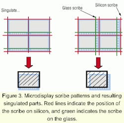
After the glass and silicon wafers are laminated together by curing the perimeter seal, the wafer-scale phase of the manufacturing process is complete. A singulation process (mechanical or laser scribing, or dicing with a saw) now separates the individual display die on the wafer laminate. Techniques such as scribing or partial sawing, which affect only the laminate outer surfaces, prevent breakage of conductors on the inner surfaces of the substrates, as well as leakage of cooling fluid into the cell interior. The singulation technique must also allow for connection to the ITO common electrode on the glass substrate and to the bond pads on the silicon substrate. This is usually accomplished by offsetting the silicon and glass scribe lines so that one substrate overhangs the other. Figure 3 shows the position of the glass scribe by a green line, and the position of the silicon scribe by a red line. The lines can be offset in a single direction, which allows bond pads on one die edge, or in two directions, allowing bond pads on two die edges. The connection to the ITO common electrode can be made anywhere along the glass overhang.
The singulated displays can be filled with LC by capillary action from a wick or a trough filled with the liquid LC material. FLCs are smectics, the more ordered of the LC phases, and hence are very viscous at room temperature. This characteristic makes possible another filling technique in which a metered amount of LC material is dispensed onto the cell, usually on the glass overhang near the fill-hole opening. The cell is then placed in a vacuum oven and temperature cycled to melt the LC and allow it to be drawn into the cell gap by capillary action. When the fill is complete, a small amount of adhesive is placed over the fill hole to seal the cell.
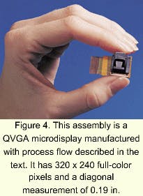
The sealed display can then be packaged by a variety of fairly well-established electronic packaging techniques. Figure 1 shows a typical packaging approach. A compliant adhesive attaches the microdisplay to a ceramic substrate attached to the end of a flexible printed circuit. Wedge-bonded aluminum bond wires connect bond pads on the microdisplay silicon to gold-plated traces on the flex. An encapsulant protects the wire bonds. Conductive adhesive connects the ITO electrode on the glass window to a pad on the flex. A conductive post or shim on the package can reduce the needed conductive adhesive thickness. The window connection can be made either by a spring clip on the window, which is subsequently wired or glued to the package, or by an indium solder connection to ITO. It is also possible to make a front-to-back connection between the glass and the silicon chip within the cell gap, allowing the window electrode to be bonded out or driven directly by a driver integrated into the display backplane. A typical end product is shown in Fig. 4.
Industry impact
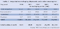
With growing microdisplay volumes, the microdisplay segment will become increasingly important to the whole semiconductor industry. The market forecast shown in the table predicts that in the year 2002, 4.5 million projection microdisplays and 25 million near-eye microdisplays will be sold.
This translates into the industry-wide consumption of about fifteen thousand 200mm wafers/month averaged across the year 2002. A microdisplay company that expected to have a significant share of this market would need to provision a manufacturing line that could produce somewhat more than a dozen laminates/hour. As an example, Displaytech has partnered with Miyota Co. of Nagano, Japan, to supplement its domestic microdisplay manufacturing capacity. Displaytech has reserved a foundry allotment and is, with Miyota, installing microdisplay capacity.
Conclusion
The wafer-level fabrication of microdisplays uses silicon wafers supplied by foundries and relies heavily on equipment sets from semiconductor tool vendors. The assembly approaches also borrow typical IC packaging techniques. Challenges specific to microdisplays include small perimeter seals, singulation of silicon laminates, and LC gap control during packaging. Microdisplay industry growth of almost 70%/year over the next few years will result in wafer and equipment buys large enough to motivate the emergence of specialized microdisplay material and tool providers.
Acknowledgments
The manufacturing process developments described here were led by Chris Berliner, Beth Ellis, and J.Z. Xue of Displaytech Inc.
References
- J. Younse, "Mirrors on a Chip," IEEE Spectrum, Vol. 30, No. 11, p. 27, Nov. 1993.
- Martin Schadt, "Photo-Alignment and Patterning of Liquid Crystal Displays," Information Display, Vol. 13, p. 14, 1997.
- P.T. Kazlas et al., "Integrated Assembly of Miniature Liquid-Crystal-on-Silicon Displays," 1997 SID International Symposium Digest of Technical Papers, Society for Information Display, San Jose, CA, p. 877, 1997.
Mark Handschy is a founder, president, and CTO of Displaytech Inc. He has served as chief scientist since the company's inception in 1985, shortly after he received his PhD in physics from the University of Colorado. At Displaytech, he has developed a number of FLC light modulators and led the development of the company's microdisplay products. Displaytech, 2602 Clover Basin Drive, Longmont, CO 80503; ph 303/772-2919, fax 303/772-2193, e-mail [email protected].
Starting wafers
8" CMOS silicon wafers, planarized by chemical mechanical polising (CMP) and with highly reflective aluminum pixel mirrors, and similarly sized ITO-coated glass wafers
Clean
The first process step is to clean the wafers. This might begin by:
Megasonic wash aqueous detergent washing with megasonics
Rinse de-ionized water rinse
Dry drying
UV/ozone UV/ozone exposure to remove residual organics
Alignment layer
A thin polymer alignment layer is applied by spin coating, and then dried and cured.
Coat
Bake
Buff
The wafer is rubbed by buffing with a cloth-covered roller, which provides the directionality needed to align the liquid crystal (LC) material.
Spacers
Spacers are small particles (1µm) that are dispersed randomly overthe surface of the wafer to create a controlled gap where the LC material will be. The spacers could alternately be applied as part of the perimeter seal.
Perimeter seal
The perimeter seal is an adhesive that ultimately will hold the LC cell substrates together. It also forms a seal around the perimeter of each individual display to eventually contain the LC material. A gap, sealed later, is left in each seal ring to allow introduction of the LC material.
Assembly
Now, the silicon substrate is ready for assembly with a similarly processed ITO-coated glass wafer which is registered with the silicon wafer, and then pressed down onto the spacers. Once in perimeter seal place, the perimeter seal adhesive is cured, bonding the substrates together into a "laminate".
Register glass wafer
Press
Cure
Singulation
The laminate is then scribed between the individual dies. Both the silicon side and the glass side are scribed. Then the laminate is separated into individual displays.
Scribe
Separate
