OIST researchers improve perovskite technology for both solar cells and LEDs
Perovskite structures have optoelectronic properties that include strong light absorption and good charge transport; these qualities make the perovskite structure particularly well-suited for the design of electronic devices, from solar cells to light sources. The accelerating progress in perovskite technology over the past few years suggest new perovskite-based devices will soon outperform current technology in the energy sector (that is, if perovskite's stability and lifetime problems can be solved).
The Energy Materials and Surface Sciences Unit at the Okinawa Institute of Science and Technology Graduate University (OIST; Okinawa, Japan) led by Yabing Qi is at the forefront of this development, with now two new scientific publications focusing on the improvement of perovskite solar cells and a cheaper and smarter way to produce emerging perovskite-based LEDs.
Increasing perovskite solar cell lifetimes
In just seven years of development, the efficiency of perovskite solar cells has increased to almost rival, and is expected to soon overtake, that of commercial photovoltaic cells, but the perovskite structure still plagued by a short lifespan due to stability issues. OIST scientists have made many steps in improving the cells stability, identifying degradation factors and providing solutions towards better solar-cell architecture.
The group's newest finding suggests interactions between components of the solar cell itself are responsible for the rapid degradation of the device.1 More precisely, the titanium oxide layer extracting electrons made available through solar energy causes unwanted deterioration of the neighboring perovskite layer.
So the researchers inserted in the solar cell an additional layer made from a polymer to prevent direct contact between the titanium oxide and the perovskite layers. This polymer layer is insulating but very thin, allowing the electron current tunnel to through while not diminishing the overall efficiency of the solar cell, and yet efficiently protecting the perovskite structure.
The lifespan of the new perovskite device was extended to more that 250 hours, still not enough to compete with commercial photovoltaic cells regarding stability, but an important step forward toward fully functional perovskite solar cells.
CVD fabrication of perovskite LEDs
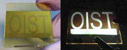
Manufacturing of perovskite LEDs is currently based on dipping or covering the targeted surface with liquid chemicals, a process which is difficult to setup, limited to small areas and with low consistency between samples. To overcome this issue, OIST researchers have created the first perovskite LED assembled via chemical vapor deposition (CVD), a gas-based fabrication method used widely throughout the optoelectronics industry.2
"CVD can achieve a uniform surface over very large areas," notes Yabing Qi.
A perovskite LED contains many layers working in synergy. First, an indium tin oxide glass sheet and a polymer layer allow electrons into the LED. The chemicals required for the perovskite layer, lead bromide and methylammonium bromide, are then successively bound to the sample using CVD. In this process, the perovskite layer is composed of nanometer-sized grains, whose dimensions play a critical role in the efficiency of the device. Finally, the last step involves the deposition of two additional layers and a gold electrode, forming a complete LED structure. The process even allows specific patterns to be formed using lithography during the manufacturing process.
"With large grains, the surface of the LED is rough and less efficient in emitting light. The smaller the grain size, the higher the efficiency and the brighter the light," says Lingqiang Meng, another researcher. "By changing the assembly temperature, we can now control the growth process and the size of the grains for the best efficiency."
The result is a flexible, thick film-like LED with a customizable pattern. The luminance currently reaches 560 cd/m2; for comparison, a typical computer screen emits 100 to 1000 cd/m2 and a ceiling fluorescent tube around 12,000 cd/m2.
'"Our next step is to improve the luminance a thousand-fold or more," says Meng. "In addition, we have achieved a CVD-based LED emitting green light but we are now trying to repeat the process with different combinations of perovskite to obtain a vivid blue or red light."
Source: https://www.oist.jp/news-center/news/2017/8/4/power-perovskite
REFERENCES:
1. Longbin Qiu et al., Journal of Physical Chemistry B (2017); doi: 10.1021/acs.jpcb.7b03921
2. Matthew R. Leyden et al., Journal of Physical Chemistry Letters (2017); doi: 10.1021/acs.jpclett.7b01093
About the Author

John Wallace
Senior Technical Editor (1998-2022)
John Wallace was with Laser Focus World for nearly 25 years, retiring in late June 2022. He obtained a bachelor's degree in mechanical engineering and physics at Rutgers University and a master's in optical engineering at the University of Rochester. Before becoming an editor, John worked as an engineer at RCA, Exxon, Eastman Kodak, and GCA Corporation.