1-µm-wide photodetector helps miniaturize silicon photonics/electronics
Researchers at Karlsruhe Institute of Technology (KIT; Karlsruhe, Germany) are making photodetectors intended for fiber-optic communications that have a base area of less than 1 µm2 without the data transmission rate being affected adversely—allowing the silicon photonic chips on which the detectors fit to be much smaller.1
In experiments, the device reached a data rate of up to 40 Gbit/s. "It is so far the smallest detector reaching this data rate," says physicist Sascha Mühlbrandt of KIT. The plasmonic internal photoemission detector (PIPED) can be integrated with electronic components on the same CMOS chip.
"Introduction of novel plasmonic components for high-speed transmission of information between electronic chips in the computer combines the advantages of electronic and optical components, while the transmission rate is comparable or even improved," says project coordinator Professor Manfred Kohl of KIT's Institute of Microstructure Technology.
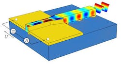
The high-performance photodetector uses surface plasmon polaritons, highly concentrated electromagnetic waves at metallic-dielectric interfaces, to combine optics and electronics in the smallest space possible. For enhancing the efficiency of light absorption and light conversion into electrical signals, charge carriers are generated at a titanium-silicon transition and taken up at another gold-silicon transition. The high rate is due to the special detector geometry: Both metal-silicon transitions are located less than 100 nm apart.
Terahertz rate wireless
The researchers consider the PIPED concept to be essential not only for future optical data transmission systems, but also for wireless data transmission. "This novel approach to detecting optical signals allows for the generation and detection of electromagnetic signals with bandwidths in the terahertz range," says Christian Koos of KIT. "Plasmonic components might be used in wireless high-speed communication and allow for transmission rates of up to 1 Tbit/s."
Source: http://www.kit.edu/kit/english/pi_2016_109_ultracompact-photodetector.php
REFERENCE:
1. S. Mühlbrandt et al., Optica (2016); doi: 10.1364/OPTICA.3.000741
About the Author

John Wallace
Senior Technical Editor (1998-2022)
John Wallace was with Laser Focus World for nearly 25 years, retiring in late June 2022. He obtained a bachelor's degree in mechanical engineering and physics at Rutgers University and a master's in optical engineering at the University of Rochester. Before becoming an editor, John worked as an engineer at RCA, Exxon, Eastman Kodak, and GCA Corporation.