Cubic gallium nitride will help cure green-LED efficiency droop
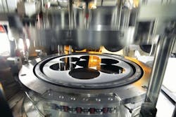
Plessey (Plymouth, England), Anvil Semiconductors (Coventry, England), and the University of Cambridge are working together to fabricate high-efficiency LEDs in cubic gallium nitride (GaN) grown on Anvil's c on silicon (3C-SiC/Si) substrates. Plessey is known for its processes to cut the cost of LED lighting by using standard silicon manufacturing techniques to make LEDs. Anvil fabricates its 3C-SiC/Si substrates by growing a thin layer of three-step cubic SiC (3C-SiC) on Si seed wafers sufficient to build active power devices.
Overcoming problems from strong internal electric fields
Cubic GaN has the potential to overcome the problems caused in conventional LEDs by the strong internal electric fields that impair carrier recombination and contribute to efficiency droop. This problem is particularly acute for green LEDs, where the internal electric fields are stronger and are believed to cause a rapid reduction in efficiency at green wavelengths known as "the green gap." The availability of cubic GaN from a readily commercializable process on large-diameter Si wafers will help to increase the efficiency of green LEDs and reduce the cost of LED lighting.
The collaboration, which is partly funded by Innovate UK under the £14m Energy Catalyst Programme, follows on from work by Anvil Semiconductors and the Cambridge Centre for GaN at the University of Cambridge, where they successfully grew cubic GaN on 3C-SiC on silicon wafers by MOCVD. The underlying 3C-SiC layers were produced by Anvil using its patented stress relief process that the company says enables growth of device-quality silicon carbide on 100-mm-diameter Si wafers.
150 mm and larger wafers
The process is readily migrated onto 150-mm-diameter and potentially larger wafers without modification, making it suitable for industrial-scale applications. Plessey has started to commercialize LEDs produced in conventional (hexagonal) GaN grown 150 mm silicon wafers using a process originally developed at The University of Cambridge. Anvil's 3C-SiC technology allows single-phase cubic GaN epitaxy growth and provides a process that is compatible with Plessey's GaN-on-Si device technology.
"The properties of Cubic GaN have been explored before, but the challenges of growing this thermodynamically unstable crystal structure have limited its development," says Colin Humphreys, director of the Cambridge Centre for GaN. "The high quality of Anvil's cubic SiC on Si substrates and our experience of developing conventional GaN LED structures on large-area wafers have enabled a breakthrough in material quality. This latest project will build on our ongoing collaboration with Plessey to deliver, for the first time, green LED devices with efficiency approaching that in blue and red LEDs."
Source: Plessey
About the Author

John Wallace
Senior Technical Editor (1998-2022)
John Wallace was with Laser Focus World for nearly 25 years, retiring in late June 2022. He obtained a bachelor's degree in mechanical engineering and physics at Rutgers University and a master's in optical engineering at the University of Rochester. Before becoming an editor, John worked as an engineer at RCA, Exxon, Eastman Kodak, and GCA Corporation.