Liquid crystal flowers can act as lenses
Philadelphia, PA--University of Pennsylvania material scientists, chemical engineers, and physicists have made another advance in their effort to use liquid crystals as a medium for assembling structures: they have created petals of a "flower" from transparent liquid crystal that radiate out in a circle from a central point--an ensemble that resembles a compound eye that can be used as a lens. Their work was published in Physical Review X (http://prx.aps.org/abstract/PRX/v3/i4/e041026).
In their earlier studies, the team produced patterns of defects in nanoscale grids and rings. The new study adds a more complex pattern out of an even simpler template: a three-dimensional array in the shape of a flower. The researchers' ongoing work with liquid crystals is an example of a growing field of nanotechnology known as directed assembly, in which scientists and engineers aim to manufacture structures on the smallest scales without having to individually manipulate each component. Rather, they set out precisely defined starting conditions and let the physics and chemistry that govern those components do the rest.
The starting conditions in the researchers' previous experiments were templates consisting of tiny posts. In one of their studies, they showed that changing the size, shape, or spacing of these posts would result in corresponding changes in the patterns of defects on the surface of the liquid crystal resting on top of them. In another experiment, they showed they could make a "hula hoop" of defects around individual posts, which would then act as a second template for a ring of defects at the surface.
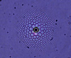
In their latest work, the researchers used a much simpler cue: "Before we were growing these liquid crystals on something like a trellis, a template with precisely ordered features," said Randall Kamien, professor in the School of Arts and Sciences' Department of Physics and Astronomy. "Here, we're just planting a seed." The seed, in this case, was a silica bead. Planted at the top of a pool of liquid crystal, flower-like patterns of defects grow around each bead.
The key difference between the template in this experiment and ones in the research team’s earlier work was the shape of the interface between the template and the liquid crystal.
In their experiment that generated grid patterns of defects, those patterns stemmed from cues generated by the templates' microposts. Domains of elastic energy originated on the flat tops and edges of these posts and travelled up the liquid crystal's layers, culminating in defects. Using a bead instead of a post, as the researchers did in their latest experiment, makes it so that the interface is no longer flat. "Not only is the interface at an angle, it's an angle that keeps changing," Kamien said. "The way the liquid crystal responds to that is that it makes these petal-like shapes at smaller and smaller sizes, trying to match the angle of the bead until everything is flat."
Surface tension on the bead also makes it so these petals are arranged in a tiered, convex fashion. And because the liquid crystal can interact with light, the entire assembly can function as a lens, focusing light to a point underneath the bead. "It's like an insect's compound eye, or the mirrors on the biggest telescopes," said Kamien. "As we learn more about these systems, we're going to be able to make these kinds of lenses to order and use them to direct light."
This type of directed assembly could also be useful in making optical switches and other shapes useful for many applications.
SOURCE: The University of Pennsylvania; http://www.upenn.edu/pennnews/news/penn-researchers-grow-liquid-crystal-flowers-can-be-used-lenses
About the Author

Gail Overton
Senior Editor (2004-2020)
Gail has more than 30 years of engineering, marketing, product management, and editorial experience in the photonics and optical communications industry. Before joining the staff at Laser Focus World in 2004, she held many product management and product marketing roles in the fiber-optics industry, most notably at Hughes (El Segundo, CA), GTE Labs (Waltham, MA), Corning (Corning, NY), Photon Kinetics (Beaverton, OR), and Newport Corporation (Irvine, CA). During her marketing career, Gail published articles in WDM Solutions and Sensors magazine and traveled internationally to conduct product and sales training. Gail received her BS degree in physics, with an emphasis in optics, from San Diego State University in San Diego, CA in May 1986.