Stacked CMOS image sensor from Sony improves on conventional back-illuminated designs
Tokyo, Japan--A new back-illuminated CMOS image sensor that layers back-illuminated structure pixels onto chips containing the circuit section for signal processing in place of supporting substrates in conventional back-illuminated CMOS image sensors has been developed by Sony. The stacked CMOS structure improves image quality with higher pixel numbers, increases imaging speed and low-light-imaging capability, and has a more compact size than traditional back-illuminated CMOS image sensors.
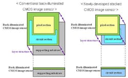
Conventional CMOS image sensors mount the pixel section and analog logic circuit on top of the same chip, which require numerous constraints when wishing to mount the large-scale circuits such as measures to counter the circuit scale and chip size, measures to suppress noise caused by the layout of the pixel and circuit sections, and optimizing the characteristics of pixels and circuit transistors.
The Sony structure layers the pixel section containing formations of back-illuminated structure pixels over the chip affixed with mounted circuits for signal processing, which is in place of supporting substrates used for conventional back-illuminated CMOS image sensors. Via the stacked structure, large-scale circuits can now be mounted on small chip sizes. Furthermore, as the pixel section and circuit section are formed as independent chips, a manufacturing process can be adopted that enables the pixel section to be specialized for higher image quality while the circuit section can be specialized for higher functionality, thus simultaneously achieving higher image quality, superior functionality, and a more compact size. In addition, faster signal processing and lower power consumption can also be achieved for the circuit chip.
Samples will be shipped beginning March 2012. The new models have been developed with Sony's "RGBW Coding" function that facilitates low noise, high-quality image capture even in low-light conditions, and the proprietary "HDR (High Dynamic Range) Movie" function achieves brilliant color even when taking pictures against bright light.
SOURCE: Sony; www.sony.net/SonyInfo/News/Press/201201/12-009E/index.html
About the Author

Gail Overton
Senior Editor (2004-2020)
Gail has more than 30 years of engineering, marketing, product management, and editorial experience in the photonics and optical communications industry. Before joining the staff at Laser Focus World in 2004, she held many product management and product marketing roles in the fiber-optics industry, most notably at Hughes (El Segundo, CA), GTE Labs (Waltham, MA), Corning (Corning, NY), Photon Kinetics (Beaverton, OR), and Newport Corporation (Irvine, CA). During her marketing career, Gail published articles in WDM Solutions and Sensors magazine and traveled internationally to conduct product and sales training. Gail received her BS degree in physics, with an emphasis in optics, from San Diego State University in San Diego, CA in May 1986.