SENSOR FUSION: AFM-IR characterizes photovoltaics at the nanoscale
MICHAEL LO, KEVIN KJOLLER, CURTIS MARCOTT, and ROSHAN SHETTY
Organic photovoltaic (PV) materials are being heavily pursued for harnessing solar power. In both private and academic sectors, major efforts are underway to prepare solar panels with the highest power-conversion efficiency at the lowest possible cost. Polymer blends of poly(3-hexylthiophene) (P3HT) and (6,6)-phenyl-C61-butyric acid methyl ester (PCBM) are a popular donor-acceptor bulk heterojunction (BHJ) that has been used for this purpose. Such material can be solution-processed before grafting onto surfaces and can yield a high η (greater than 5%).
In a typical organic solar cell, P3HT and PCBM are not miscible and are eventually phase-separated into microdomains.1 The details of this process are critical to the long-term stability and performance of the PV materials. Covalently linking PCBM to polymeric P3HT would yield small feature sizes thought to be advantageous for long-term stability but the performance suffers, as the P3HT backbone is believed to conduct charges poorly.2 Atomic-force microscopy (AFM) and transmission electron microscopy have been used to characterize the morphology of these PV films at high spatial resolution, but chemical information is not readily available at the nanoscale. Here, we correlate topological features to local chemical spectroscopy on P3HT and PCBM-doped P3HT films using a novel AFM-infrared (AFM-IR) technology.
Introduction to the nano-IR
Infrared spectroscopy is one of the most practiced analytical measurement techniques in industrial and academic R&D laboratories. Unfortunately, diffraction physics limit its spatial resolution to a few to tens of microns, depending on the optics involved and the wavelength of the light. This major limitation has now been eliminated by Anasys Instruments with the development of the AFM-IR platform. This spatial-resolution breakthrough is obtained via a novel technique that uses a nanoscale probe from an AFM that acts as the IR-absorbance detector. The nature of the IR-absorbance detection results in simultaneous measurements of nanoscale mechanical properties and nanoscale morphology, along with information on the chemical composition. The instrument also has integrated nanoscale thermal-property mapping, resulting in a multifunctional tool that provides nanoscale structural, chemical, mechanical, and thermal properties.
At the heart of the AFM-IR platform is patented technology based on a combination of AFM and IR spectroscopy, a technique pioneered by Alexandre Dazzi from the Laboratoire de Chimie Physique (CLIO), Université Paris-Sud (Orsay, France).
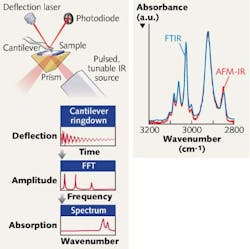
The AFM-IR system uses a pulsed, tunable IR source to excite molecular vibrations in a sample that has been mounted on an IR transparent zinc selenide (ZnSe) prism. This creates an illumination configuration similar to conventional attenuated-total-reflectance (ATR) spectroscopy. The system’s IR source is continuously tunable from 1200–3600 cm-1, covering a broad range of the mid-IR spectrum. As the sample absorbs radiation it heats up, leading to rapid thermal expansion that excites resonant oscillations of the cantilever. The induced oscillations decay in a characteristic ring-down (see Fig. 1). The ring-down is Fourier-transformed to extract the amplitudes and frequencies of the oscillations. Measuring the amplitudes of the cantilever oscillation as a function of the source wavelength creates local absorption spectra; the oscillation frequencies of the ring-down are related to the mechanical stiffness of the sample.
Users of the AFM-IR can quickly survey regions of a sample via AFM imaging and then rapidly acquire high-resolution chemical spectra at selected regions on the sample. Polymer spectra acquired with the AFM-IR system have demonstrated good correlation with bulk Fourier-transform IR (FTIR) spectra.
This allows the researcher to import an individual AFM-IR spectrum into commercial IR databases, where they can be digitally searched in order to chemically identify the materials at the specific sample locations measured. Alternatively, the IR source can be tuned to a single wavelength to map compositional variations across the sample surface.
In addition to its ability to provide high-resolution IR spectra, the AFM-IR system provides information on the mechanical properties of the sample. This is accomplished by monitoring the frequency of the fundamental or higher resonant modes of the cantilever. This is analogous to the contact-resonance method used for a number of years in the AFM community. The contact resonant frequency of the cantilever correlates to the stiffness of the sample and can be used to map the modulus of the sample qualitatively.
The AFM-IR platform can also perform nanoscale thermal analysis using novel AFM cantilevers that incorporate a resistive heating element into the end of the cantilever. Using these cantilevers in combination with the system allows the local measurement of the transition temperature of materials at a single point or an array of points across a sample. This allows identification or mapping of the amorphous/crystalline content, stress, extent of cure, and other material properties that can be characterized by the transition temperature of the material.
Measurement of P3HT and PCBM-doped P3HT
The AFM-IR technique is ideal for measuring polymeric samples in which there are local material variations. The sampling system requires the material of interest to be deposited as a thin film on a ZnSe prism. This prerequisite is satisfied by drop-casting the materials from solution directly onto the prism.
Not all surface features on the same AFM image share the same IR-absorption characteristics. In one example, an area of interest has small protrusions on the order of a few microns in size.
Normalized point-and-click IR spectral acquisition reveals that only some locations have slightly broadened absorption characteristics—that is, a long absorption tail (Spectrum 10)—and a less defined shoulder near 1500 cm-1. The other locations yield spectra similar to the bulk P3HT material. Near points correlating to spectra 12 to 14, the broadened absorption appears to be away from the height feature.
To enhance the spectral analysis, the area near the spectra labeled 12 to 14 was rescanned with a high spatial resolution producing a corresponding image; a spectral array acquisition about the region was collected immediately afterward. Here, each spectrum is taken about 100 nm apart and spectral changes are seen within the same-length scale (from second to third and from fifth to sixth spectra). As the shoulder around 1500 cm-1 disappears and reappears (at the arrows), the signal near 1380 cm-1 appears to broaden. With the AFM-IR, these IR spectral changes can be seen at an unprecedentedly high spatial resolution.
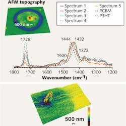
Phase separation of PCBM and P3HT is commonly observed in such PV blends. In an example AFM image of a heat-treated P3HT-PCBM sample, a defect can be seen on the surface of the sample (see Fig. 2). The localized IR spectra pertinent to surface features are shown directly below the image. When the AFM-IR spectra are compared to the AFM-IR spectra for the pure components, local variations are distinguished. The methylene bending modes at 1444 and 1432 cm-1 correspond to the P3HT and PCBM, respectively. The 1444 cm-1 band also contains a contribution from an overlapping ring semicircle stretching mode. The corresponding spectrum for the yellow hash mark appears to have both components. At the outer ring (red mark/spectrum 1), the peak at 1732 cm-1 (PCBM) is small and the component at 1444 cm-1 (P3HT) dominates. At both green and purple hash marks (spectra 3 and 4), the band near 1432 cm-1 is mainly contributed by PCBM. Finally, the sharpness of the band at 1432 cm-1 and a stronger 1732 cm-1 signal suggest that the lobe at the center is mostly PCBM. By combining the AFM and IR into a single instrument, the topological information is readily correlated with the local chemical analysis. This data suggests that there is local phase-separation of PCBM and P3HT within this surface defect.In addition, the stiffness of the surface defect relative to that of the P3HT-PCBM blend can be imaged using the AFM-IR. Under the exposure of a continuously pulsing IR laser radiation at 1450 cm-1 (other overlapping wavenumbers for both materials can also be used), the contact frequency of the cantilever is traced continuously as the AFM tip rasters across the sample. Here, the bulk material (yellow/orange) appears stiffer than most of the interior areas of the defect (green).
Linking diverse material properties
Such data demonstrate the strong capability of the AFM-IR in analyzing a set of photovoltaic materials at high spatial resolution. The topological features can be conveniently linked to its corresponding chemical IR signatures. A spatial resolution of 100 nm can be readily achieved in applications where domain boundaries are unknown. Local phase separation of materials is identified by comparing local AFM-IR spectra at the defect sites with the bulk spectra of the pure components. In addition, the relative contact frequencies surrounding the defect are mapped simultaneously with the corresponding topology.
REFERENCES
1. Y. Yang et al., J. Mater. Chem., 17, 3126–3140 (2007).
2. S. Holdcroft et al., Poly. Chem., 1, 708–719 (2010).
Michael Lo, Kevin Kjoller, and Roshan Shetty are at Anasys Instruments, Santa Barbara, CA, www.anasysinstruments.com; e-mail: [email protected]. Curtis Marcott is at Light Light Solutions, Athens, GA.

