PHOTONIC FRONTIERS: QUANTUM DOTS: Quantum dots address a range of new applications
Many key advances in diode lasers since their invention in 1962 stemmed from improvements in optical and electronic confinement. Double heterojunctions enabled continuous-wave operation at room temperature and eventually earned Herbert Kroemer and Zhores Alferov the 2000 Nobel Prize in physics. Quantum wells followed, further improving diode laser performance and eventually becoming standard in commercial lasers.
Quantum dots are logical extensions of quantum wells, confining electron-hole pairs in a tiny three-dimensional (3D) volume instead of a thin layer. Quantum dots can be viewed as artificial atoms with the confinement geometry and the semiconductor material combining to determine their optical and electronic properties. Designers can use that flexibility to engineer semiconductor devices with properties unavailable from conventional compound semiconductors, including extremely low laser thresholds, and broader emission and absorption bandwidths.
Quantum dot challenges
The two main approaches to producing quantum dots are epitaxial growth in compound semiconductor devices and colloidal growth in solution. Here we focus on epitaxial growth of quantum dots for use in semiconductor diodes.
Epitaxial growth and organization of 3D nanostructures is challenging. Epitaxy is good for growing the atomic-scale layers used in quantum wells, but the patterning and etching techniques needed for lateral confinement “have not progressed to the atomic scale as quickly, and as a result, development of lasers with higher order quantum confinement has progressed more slowly,” writes James Coleman of the University of Illinois (Urbana, IL) in a tutorial paper.1
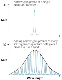
The simplest approach to fabricating quantum dots in a semiconductor device is self-arrangement. The process begins by growing a few thin layers with internal strain on a surface, and continues until strain reaches a point at which isolated islands of semiconductor with a different composition begin growing at random sites. Further growth of those islands produces quantum dots, self-arranged in a range of sizes at random spots on the surface. Those variations produce a linewidth of 20–30 meV, compared to the linewidth of a single quantum dot, which is desirable for some applications (see Fig. 1). The self-assembled dots, however, cover only a few percent of the surface, so the emitting volume is much smaller than a quantum well.
An alternative is to pattern the surface so quantum dots grow uniformly across the area. This gives much more uniform properties, reducing linewidth to 1 meV, and can cover more of the surface with dots, offering stronger emission. However, the patterns require extremely small and tightly spaced structures, which are hard to fabricate with current photolithographic technology, but Coleman notes that such patterns should become easier to make as semiconductor electronics pushes fabrication technology to higher resolution.
Quantum dots also must compete with established technology. “The world is reasonably happy with quantum well devices,” says Pallab Bhattacharya at the University of Michigan (Ann Arbor, MI). So quantum-dot developers need to target application niches poorly served by quantum wells, or offer big improvements, to justify major investment in new technology. They have already found some applications.
Emitters and amplifiers
One such application is making 1.3 µm lasers on gallium arsenide (GaAs) rather than the usual indium phosphide (InP), says Bhattacharya. Quantum-dot lasers can accommodate strain better than quantum wells, allowing InGaAs/GaAs lasers to be stretched to the 1.3 µm band. Gallium arsenide is less expensive, and the characteristic temperature of a GaAs quantum-dot laser is much higher than equivalent quantum well lasers on InP, reducing wavelength drift with temperature and thus avoiding the need for thermoelectric cooling for wavelength stabilization and allowing faster direct modulation.
Quantum dots also have found success in optical amplifiers, where broad bandwidth is highly desirable. By stacking quantum-dot layers, QD Laser (Kawasaki, Kanagawa, Japan) has made amplifiers with 120 nm bandwidth—triple that of conventional single-band erbium-doped fiber amplifiers—and output of 100 mW. QD Laser, a joint venture of Fujitsu and Mitsui that specializes in quantum-dot technology, also makes quantum-dot distributed-feedback lasers that can be frequency doubled to 532 nm.
Cutting-edge laboratory lasers
Quantum-dot research, meanwhile, is pushing the cutting edge of diode laser performance in the laboratory. The tight confinement in quantum dots gives them inherently low laser thresholds. The lowest reported thresholds have been only a few nanowatts for optical pumping of photonic crystal nanocavities.2 That’s far below the thresholds for electrical pumping, which have been on the order of 100 µW for both edge-emitting diodes and vertical-cavity surface-emitting lasers (VCSELs). Yet electrical pumping is preferred for many applications where low thresholds are sought, such as optical interconnections on high-performance computer chips.
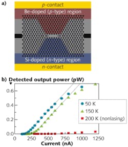
Now Jelena Vuckovic’s group at Stanford University (Stanford, CA) has achieved record-low threshold currents of 181 nA at 50 K and 287 nA at 150 K (see Fig. 2). The intrinsic layer of the group’s electrically excited lateral p-i-n diode laser was narrowed to 400 nm in the active region where the current passed through photonic-crystal nanocavities containing three layers of InAs quantum dots embedded in GaAs. The group found that much of the current leaks into the substrate and estimates that the threshold could be reduced to 70 nA if the leakage could be stopped.3Direct green diode lasers
Bhattacharya’s group is tackling another difficult problem: direct diode lasers emitting green light for applications including picoprojectors and displays. It requires adding enough indium to InGaN diode lasers to shift the emission to the 530 nm range while maintaining good laser performance. Other developers are coming close with quantum-well lasers. Prospects for green quantum-dot lasers “were totally unexplored,” says Bhattacharya.
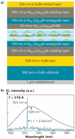
Now the group has succeeded in demonstrating the first electrically-pumped InGaN quantum-dot lasers. It grew self-organized quantum-dot laser heterostructures on the C plane of GaN substrates using the structure shown in Fig. 3a. Figure 3b compares the spectrum of pulsed laser emission at 524 nm, with 0.7 nm linewidth, to the broader fluorescence spectrum. In a paper in press at Applied Physics Letters, the group reports a threshold current of 1.2 kA/cm2 at 278 K, with slope efficiency 0.74 W/A, and wallplug efficiency of 1.1% at drive current of 1.3 kA/cm2.4 Those results are comparable to others reported earlier from quantum-well lasers.5Infrared detectors and solar cells
Like other semiconductor diodes, quantum-dot devices can absorb and detect photons as well as emit them. Coleman says that the variation in quantum-dot transition energy, a liability for lasers in some applications, may benefit detectors because it enhances their sensitivity range.
Quantum dots are particularly attractive for infrared detectors because they can operate at higher temperatures then conventional types, which require cooling. Room-temperature InAs quantum-dot detectors have been demonstrated in the important 3–5 µm band, which generally requires cooling.6 Recently, InAs quantum-dot detectors operating in the 3–5 µm and 8–12 µm bands have been stacked on top of each other to span 4–11 µm.7
Fabrication of germanium quantum dots on silicon opens other possibilities. Their operating band spans the 1.31 and 1.55 µm fiber-optic bands, and is compatible with silicon microelectronics.8 That’s very attractive for optical interconnections on silicon chips.
Solar cells have been demonstrated using quantum dots, but the application requirements and economics differ greatly from those for detectors and developers have focused on colloidal quantum dots, which can cover large areas at low cost. Work remains in the development stage, but quantum dots have valuable properties, such as the ability to generate two or three electron-hole pairs when illuminated by short-wavelength light.9
Outlook
So far, quantum dots have been most successful in niche applications, where their advantages are compelling enough to create new markets or displace other technologies. Displacing well-established technologies in broader markets has been tough, both because older technologies such as quantum wells had a head start and because quantum dots have their own limitations. Fabricating, manipulating and organizing quantum dots in well-controlled ways are inherently challenging because of their nanoscale sizes.
Meanwhile, researchers are pushing forward with new applications. Yasuhiko Arakawa’s group at the University of Tokyo (Tokyo, Japan) has demonstrated laser oscillation in a single semiconductor quantum dot coupled to a photonic-crystal nanocavity.10 Unidirectional emission has been demonstrated from a single quantum dot coupled to a nanoscale Yagi-Uda antenna.11 Single-photon emission has also been demonstrated.12 And a pair of InAs quantum dots have been used to demonstrate the control of optical entanglement of their spins with ultrafast lasers.13 Those impressive demonstrations could point the way to future quantum-dot applications.
REFERENCES
1. J.J. Coleman et al, “Semiconductor Quantum Dot Lasers: A Tutorial,” J. Lightwave Technol., 29, 499 (Feb. 15, 2011).
2. S. Strauf et al., “Self-tuned quantum dot gain in photonic crystal lasers,” Phys. Rev. Lett., 96, 127404 (2006).
3. B. Ellis et al., “Ultralow-threshold electrically pumped quantum dot photonic-crystal nanocavity laser,” Nat. Photon. online; doi: 10.1038/NPHOTON.2011.51 (Apr. 24, 2011).
4. M. Zhang et al., “A InGaN/GaN Quantum Dot Green (lambda=524 nm) Laser,” Appl. Phys. Lett., 98, 221104; doi:10.1063/1.3596436 (in press; 2011).
5. J. Hecht, “Photonic Frontiers: The quest for practical green laser diodes,” Laser Focus World, 46, 12, 65–67 (December 2010).
6. M. Razeghi, “Quantum-dot IR photodetectors get ‘hotter’,” Laser Focus World, 43, 12, 75–76 (December 2007).
7. W.-H. Lin et al., “Broadband Quantum-Dot Infrared Photodetector,” IEEE Photon. Technol. Lett., 22, 13, 963 (July 1, 2010).
8. O.P. Pchelyakov et al., “Ge/Si heterostructures with coherent Ge quantum dots in silicon for applications in nanoelectronics,” Semicon. Sci. Technol., 26 014027; doi:10.1088/0268-1242/26/1/014027 (2011).
9. R. Ellingson et al., “Highly Efficient Multiple Exciton Generation in Colloidal PbSe and PbS Quantum Dots,” Nano Lett., 5, 5, 865; doi:10.1021/nl0502672 (2005).
10. M. Nomura et al., Nat. Phys., 6, 279 (2010).
11. A.G. Curto et al., “Unidirectional emission of a quantum dot coupled to an optical nanoantenna,” Science, 329. 930 (2010).
12. E. Stock et al., “High-speed single-photon source based on self-organized quantum dots,” Semicond. Sci. Technol., 26, 014003; doi:10.1088/0268-1242/26/1/014003 (2011).
13. D. Kim et al., “Ultrafast optical control of entanglement between two quantum-dot spins,” Nat. Phys., 7, 223–229 (2011).
About the Author
Jeff Hecht
Contributing Editor
Jeff Hecht is a regular contributing editor to Laser Focus World and has been covering the laser industry for 35 years. A prolific book author, Jeff's published works include “Understanding Fiber Optics,” “Understanding Lasers,” “The Laser Guidebook,” and “Beam Weapons: The Next Arms Race.” He also has written books on the histories of lasers and fiber optics, including “City of Light: The Story of Fiber Optics,” and “Beam: The Race to Make the Laser.” Find out more at jeffhecht.com.


