TERAHERTZ DETECTORS: Air bridge improves terahertz detector response time
SARA CIBELLA, ROBERTO CASINI, ALESSANDRA DI GASPARE, and MICHELE ORTOLANI
Terahertz imaging is a very promising technology for applications in security screening, nondestructive testing, and biomedicine. Like millimeter waves used by radars and body scanners, radiation with frequency between 0.6 and 6 THz can be used to image objects through opaque dielectric materials, such as clothing, envelopes, and packages. In addition, it can provide sub-millimeter resolution in the far-field, thanks to its much shorter wavelength of 50–500 μm. What makes terahertz radiation really different from millimeter waves, however, are the terahertz spectral signatures of gases, biomolecules, and solids and the peculiar frequency dependence of the terahertz absorbance of liquid water.
These spectral properties can provide strong imaging contrast among different substances that cannot be achieved by infrared or millimeter waves. It is possible, therefore, to combine the imaging capabilities and the spectral sensitivity of terahertz radiation to obtain "false-color terahertz images" (spectroscopic imaging), allowing both object detection and substance identification. System compactness, complexity, and cost must, however, be improved for commercial applications of terahertz spectroscopic imaging.
Several laser-based technologies for broadband terahertz spectroscopy have been developed that have short acquisition times of a few seconds. This is enabled by the very high detector sensitivity achieved by coherent detection of difference-frequency signals generated by two narrowband tunable infrared lasers (photomixing), or by time-domain analysis of sub-picosecond terahertz pulses generated by modelocked lasers impinging on ultrafast photoswitches. However, adding multipixel imaging capabilities to these systems is not easy, as the laser beam needs to be multiplexed onto arrays of photoswitches or photomixers; alternatively, the terahertz beam from a single transmitter needs to be steered, electronically or mechanically.
A different approach to terahertz imaging uses narrowband terahertz sources delivering output powers on the order of 1 mW for flood-illumination of the target, with the transmitted/reflected radiation focused onto multipixel focal-plane arrays (FPAs). Compact point-like sources are now available, such as terahertz quantum-cascade lasers (QCLs) in the 2–5 THz range and electronic amplifier-multiplier chains (AMCs) in the 0.2–1.2 THz range.1,2 Instead of acquiring full terahertz spectra, a multispectral capability can still be implemented in narrowband imaging with FPAs by illuminating the target with a number of sources or by fine-tuning of the emission frequency. The multispectral information can be retrieved from the FPA by demodulation at the detector level.
Video-rate imaging at a single terahertz frequency has been demonstrated by coupling QCLs to commercial infrared FPAs composed of thermal sensors (microbolometers or pyroelectric detectors). Since these detectors are based on relatively large-area (typically 50 × 50 μm) energy absorbers, each pixel displays a time constant above 10 ms. This is not a problem for video-rate image acquisition, as the single pixel response can still be electronically sampled at high speed; however, the slow thermal time constant prevents the use of more sophisticated read-out schemes, such as multispectral demodulation. For this reason, among others, our group at CNR-IFN in Rome is developing terahertz detectors with microsecond response times fabricated by lithography, anticipating future integration into monolithic FPAs.
Air-bridge terahertz detectors
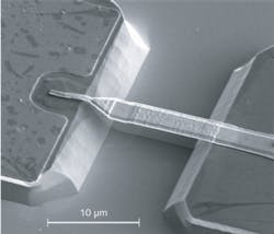
If we ignore for the moment the issue of amplifier bandwidth, the intrinsic detector response time is set by its conductance (should be high) and capacitance (should be low), and is therefore a function of materials and fabrication techniques. A shorter detector response time can be obtained by either active-region miniaturization or isolation of the active region from the inert structure (electrical contacts, substrate and so on). Since air (or vacuum) is the best medium for electrical and thermal isolation, it follows that locating the active region of the detector on a micrometric air bridge is an attractive option. This approach holds for both thermal detectors, normally considered in terms of thermal conductance and capacitance, and terahertz rectifiers, where the intrinsic response time must be shorter than the electromagnetic-wave period (1 ps for 1 THz). Schottky barrier diodes (SBDs) are in this class of detectors (see Fig. 1).
In two detector prototypes produced at CNR-IFN, micrometric air bridges have a shorter detector response time than that of commercially available devices. In both cases, coupling terahertz radiation with wavelengths of 50–500 μm to the micrometric active region is achieved by fabricating an on-chip planar terahertz antenna. A silicon-substrate lens then focuses the incoming beam into the antenna. The air bridge and the active region are located between the antenna feeds. The device layout is a two-dimensional detector array with enough space left on-wafer for interconnects and preprocessing electronics, which will be added in the future. Currently, single pixels are diced from the array, mounted in packages with the substrate lens, and tested with external electronic circuitry.
Superconducting hot-spot air-bridge bolometer
The superconducting hot-spot air-bridge bolometer (SHAB) consists of a niobium (Nb) air bridge 1 μm wide and 15 μm long suspended between the feed points of a logarithmic spiral antenna. Below the superconducting critical temperature Tc ≈ 8.2 K, a DC current bias produces a normal-state region (called a hot spot) where the local temperature is higher than Tc at the center of the bridge. This is possible because of the high thermal isolation of the suspended part of the bridge from the thermal bath (the substrate). As a result, the bridge features a nonzero value of the resistance, which can be set close to the antenna impedance of 75 Ω. The incident terahertz radiation induces a time-varying current in the antenna, dissipating power in the impedance-matched bridge and increasing the size of the hot spot, hence the quasi-static value of the resistance. The response time of the detector is thus related to the thermalization time of the hot spot and is given by b = C/G, where C is the thermal capacitance and G the thermal conductance of the bridge.
We have developed a fabrication process to obtain highly reproducible values of G and C. First, a 50 nm layer of Nb is deposited on top of a 75 mm diameter silicon wafer coated with 100 nm of silicon nitride (SiNx) providing both electrical isolation and mechanical stiffness to the bridge. The lithographic antenna is produced by 20 nm-titanium (Ti)/200 nm-gold (Au) evaporation and lift-off. Electron-beam lithography is then used to define the bridge by chromium (Cr) masking and reactive ion etching of the remaining Nb film. A further lithography step encapsulates the Nb stripe in hydrogen silsesquioxane to protect it for the final deep isotropic etching of the Si substrate, in which approximately 3 μm of Si are removed underneath the Nb/SiNx bridge.
Short 200 ns pulses emitted by a pulse-driven QCL emitting at 4.4 THz allowed us to estimate the SHAB response time to be τ = 5.8 ± 0.2 μs from an exponential fit of the principal rise and decay times (see Fig. 2). By connecting the SHAB to a lock-in amplifier and using the QCL drive signal as the reference fR, one can compare the SHAB output bandwidth to that of a pyroelectric detector. The preamplifiers of both detectors were set to have a noise level of 1 μV at 30 Hz; the pyroelectric response rolls off above 30 Hz and it is smaller than the SHAB response by a factor of 103 at 30 Hz, consistent with the pyroelectric noise equivalent power (NEP) of ≈10-9 W/Hz0.5. The SHAB response measured with the lock-in is almost constant up to 100 kHz and then starts to roll off due to nonoptimized parasitic capacitances in the cryostat wiring. The SHAB NEP is 10-13 W/Hz0.5. We conclude that the SHAB can provide almost three decades of frequency range with constant response (100 Hz–100 kHz), which allows multichannel acquisition with a single pixel and multispectral demodulation.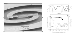
Air-bridge Schottky barrier diode
The SBD is the most used semiconductor device in coherent (heterodyne) systems operating at frequencies beyond 0.5 THz. The main reason is that the nonlinear current-voltage characteristics depend (to first order) only on majority carrier transport; hence, recombination rates are unimportant for the determination of the high-frequency cutoff. As a result, temperature has only a minor effect on the SBD properties, allowing it to work at room temperature—a relevant feature for applications. The nonlinear properties derive from electrons crossing a single metal/semiconductor interface; therefore, the SBD displays very low capacitance. The SBD transmission coefficient for electrons in the semiconductor has an exponential dependence on the voltage applied at the diode terminals (thermionic emission). The electric field oscillating at the radiation frequency is applied to the barrier region through the antenna and it asymmetrically changes the transmission coefficient within one radiation cycle, producing a nonsinusoidal, non-zero-average output current.
To achieve fast variation of the barrier potential at terahertz frequencies, the parasitic RC cutoff frequency has to be very high (above 3 THz); hence it is crucial to use high-mobility III-V semiconductors—gallium arsenide (GaAs), indium gallium arsenide (InGaAs), or indium phosphide (InP)—for low series resistances, and to fabricate the diode with sub-micron dimensions to ensure low junction capacitance. Once more, it is necessary to minimize parasitic current paths by fabricating an air bridge to physically decouple the anode (metal) and the cathode (semiconductor) contacts (see Fig. 3).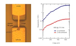
We have fabricated monolithic arrays of SBDs on n-GaAs and are experimenting on the anode geometry by defining different diode types on the same wafer with trilayer electron-beam lithography (EBL). Our process starts with the cathode definition by optical lithography, Ni/Au/Ge evaporation, and thermal annealing. T-section anodes with air-bridge contacts are then defined by EBL and Ti/Au evaporation. The trilayer resist allows us to selectively suspend or contact the different portions of the Ti/Au film, and hence to shape the 3D anode geometry. Finally, the mesa areas are protected from wet substrate removal, which suspends the bridge and isolates the diodes among each other. The experimental determination of τ is difficult due to the lack of terahertz network analyzers, but a lower bound of τ = 3.7 × 10⁻¹² s was derived from the observed rectification of a 270 GHz free-space radiation beam. In principle, the SBD output signal can be demodulated up to tens of gigahertz with appropriate amplifier design.
REFERENCES
1. M.S. Vitiello et al., "Terahertz quantum cascade lasers with large wall-plug efficiency," Appl. Phys. Lett., 90, 191115 (2007).
2. www.virginiadiodes.com
Sara Cibella, Roberto Casini, Alessandra Di Gaspare, and Michele Ortolani are researchers at the Institute for Photonics and Nanotechnology of the National Research Council of Italy (CNR-IFN) in Rome, Italy; e-mail [email protected]; www.ifn.cnr.it.