TECHNOLOGY REVIEW 2010: Scientists and engineers: A vital alliance
The quantity and quality of innovation in photonics this past year have been enormous, with many interesting achievements being the ones less publicized.
It's easy enough to sort light into "categories:" ultraviolet, visible, infrared; red, green, blue; short-, mid-, and long-wave IR; and the like. Photonic devices are not so easy. It's tempting to file this past year's many innovations in photonics into traditional categories such as imaging, light sources, and so on. But for any sort of review, which inevitably calls for the barest skimming of the year's many accomplishments, perhaps it makes sense to sort things some other way—in part because so many of these technical achievements each are based on not just one but many aspects of photonics.
Wavelength-scale photonics
One of the qualities that makes light so useful is its small wavelength—enabling sharp imaging, ultrahigh-speed communications, and, in some cases at least, compact hardware. More and more photonic devices now are being created that take advantage of light's wave properties in a deeper way, having physical structures with features from a few wavelengths down to much less than a wavelength in size.
A version of the much-hyped metamaterial invisibility cloak, for example, has been fabricated that works well in three dimensions at optical wavelengths; previously, only 2D versions have been possible in the optical region (see Fig. 1).1 Using laser lithography, scientists at the Karlsruhe Institute of Technology (Karlsruhe, Germany) and Imperial College London (London, England) created a 3D "woodpile" polymer/air photonic crystal (PC) with a tailored filling fraction and used it to hide a bump in a gold reflector (although such a cloak does not sound very versatile, it or a variation of it could become a useful tool in combination with other wavelength-scale structures). The cloak is notable in that it operates over a very large bandwidth of unpolarized light from 1.4 to 2.7 μm wavelengths at angles up to 60°.
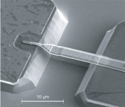
A subwavelength microcavity laser created by researchers at the Institute for Quantum Electronics at ETH Zurich (Zurich, Switzerland) has a resonator cavity consisting of two half-circle-shaped gold capacitors with radii of 10 μm that are connected by a 10 μm link acting as an inductor; the result is an effective mode volume smaller than that for any previous electrically pumped microcavity laser. The quantum-cascade gain region is 8 μm thick and lases at 207 μm. Future lasers of this sort could have mode volumes that are even smaller and that emit in the near-IR region, say the researchers.
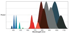
White LEDs that emit a warm-white light are much in demand but have luminous efficiencies lower than their cool-white counterparts. Lighting researchers from Bilkent University (Ankara, Turkey) and Nanyang Technological University (Singapore) have developed a warm-white LED with a nanocrystal quantum-dot (QD) phosphor that has a luminous efficacy higher than that for the best of previous warm-white phosphors. The QDs have a cadmium selenide core and a zinc sulfide shell coated with long-chain amine caps, and emit green, yellow, and orange light. When they are integrated with a standard gallium-nitride-based blue LED, the result is a pleasing light with a color-rendering index of about 90 and a color temperature below 3000 K. The quantum dots themselves have a record-high luminous efficacy of optical radiation exceeding 350 lm/W (note that this is a figure for the phosphor, not the entire LED).
Light striking a surface with the right structure can become surface plasmons—coherent oscillations of electrons on a metal surface, providing yet another way to manipulate light. Aiming to improve the performance of organic photovoltaic (PV) cells, researchers at Lehigh University (Bethlehem, PA), the Chinese Academy of Sciences and Tsinghua University (both of Beijing, China) and the National Science Foundation (Arlington, VA) have designed and simulated a polarization-independent nanopatterned surface with an active layer of nanohole-perforated silver that supports short-range surface-plasmon-polariton modes.2 Their calculations show a boost in PV performance between 39% and 112%.
Putting light to work
While many inventions are fascinating in their own right, and many others appear to have a practical future ahead of them, there are some advances in photonics that, even if they're in an early stage, seem headed for plenty of use (not that these are the only photonics innovations that could be valuable to the working world).
Femtosecond-laser micromachining has advantages over micromachining with longer-pulse or continuous-wave lasers: Rather than melt or vaporize a substance, a femtosecond laser can dissociate chemical bonds, causing very little peripheral damage and also allowing transparent materials to be machined. While beams with Gaussian intensity profiles are typically used, researchers at the Université de Franche-Comté (Besancon, France) and Macquarie University (New South Wales, Australia) have been using Bessel beams instead (created by a phase mask that generates a "virtual axicon"). This allows them to machine taper-free microchannels in glass that have aspect ratios up to 40 and diameters down to 2 μm (see Fig. 2). In fact, they later found they could do even better.3 "We have shown that a single laser shot is enough to drill a very long nanochannel, with aspect ratio up to 100:1," says François Courvoisier, one of the researchers, noting that the technique is capable of drilling periodic nanostructures 200 nm in diameter. The group will present these results in an invited talk at Photonics West 2011.Engineers at Pranalytica (Santa Monica, CA), Infrasign (Fremont, CA), and the University of California–Los Angeles have developed a laser-based system that can recognize trace quantities of an explosive substance—in this case, TNT—at distances up to 150 m with a signal-to-noise ratio up to about 70.4 The potential problem object is illuminated with light from a tunable carbon dioxide laser; light at 10.653 μm is absorbed by the TNT, causing a rise in blackbody radiation; tuning to 10.591 μm shows a scene without absorption by TNT, allowing a difference to be taken and resulting in an unambiguous determination of the target. A first prototype was deployed, with results that indicate a potential for explosives detection several orders of magnitude better than that for techniques available today. The use of a high-power room-temperature tunable quantum-cascade laser (QCL) at the same wavelengths could result in a device to screen people and their belongings at airports for explosives and explosive residues.
Fiber-based supercontinuum sources, such as those pioneered by Fianium (Southampton, England), provide single-lateral-mode white light valuable for spectroscopy, microscopy, and forms of optical metrology. Now, scientists at the University of Southampton (Southampton, England) and the Central Glass & Ceramic Research Institute (Kolkata, India) have put together a master-oscillator-power-amplifier pumped supercontinuum source that produces a highest-ever average power of 39 W over a relatively uniform wavelength range that spans 0.4 to 2.25 μm.5 A 2 m long PC fiber with a 4.4 μm diameter core is subjected to 21 ps input pulses at a 114.8 MHz repetition rate. With a fiber endcap, shorter fiber lengths could be used, reducing absorption losses, say the researchers.
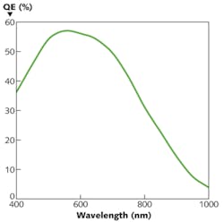
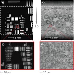
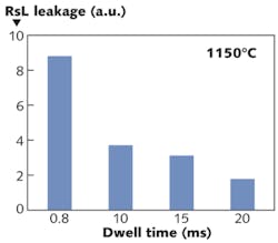
A new type of microscope, called a holographic scanning microscope, created at the California Institute of Technology (Pasadena, CA) greatly increases field of view (FOV) while maintaining a high resolution (see Fig. 3). It does this by illuminating the sample with a holographically projected light-spot grid of 200 × 40 spots of 532 nm laser light, which is scanned to produce a FOV of 6 × 5 mm, acquiring the entire image in 2.5 s. The spot size of 0.74 μm determines the resolution of 1.5 μm. The first prototype did not contain focus feedback; adding that, plus reducing scan jitter, will improve future versions. Uses will include digital pathology, where a microscope slide is imaged and digitized; and direct imaging and examining of blood or pap smears, where a wide field-of-view is helpful for diagnosis, says Jigang Wu, one of the researchers.Photoluminescence imaging of silicon has been developed to speed the inspection of solar cells. Patented by researchers at the University of New South Wales (Sydney, Australia) and offered by spinoff company BT Imaging, the technology is now being used worldwide by solar-cell manufacturers. Silicon bricks (240 × 15.6 mm in area), as-cut wafers, and fully processed solar cells can be measured. The imaging is fast: Wafers can be scanned with a throughput of up to 2400 wafers per hour. The technology is on the verge of being adopted for inline monitoring in PV manufacturing and may be used in the future in the semiconductor and LED industries (see page 35).
Many ways to use optical fiber
Solid-core PC fibers don't guide light via total internal reflection; instead, any light guiding happens strictly through the presence of a bandgap. Solid-core PC fibers are now in existence that have bandgaps up to an octave; created by a group at the University of Sydney (Sydney, Australia), the fibers have inclusions that each consist of a ring of high refractive index surrounding a circular region with a lower refractive index. As a result, the modal cutoffs cluster at particular wavelengths, greatly broadening the bandgap. In one example presented at the OSA's Frontiers in Optics 2010 (FiO; Rochester, NY, Oct. 24-28, session FTuW2), a polymer fiber has a transmission band extending from 550 to 1720 nm (with two narrow interruptions due to higher-order modes of the inclusions at 1050 and 1170 nm).
Also at FiO 2010 (session FTuW1), John Ballato of Clemson University (Clemson, SC) discussed progress on semiconductor core glass-clad optical fibers, concentrating on research going on at Clemson and Northrop Grumman Space Technology (Redondo Beach, CA). Such fibers are potentially useful in IR power delivery, as well as nonlinear fiber-optics. Crystalline unary (silicon and germanium) and binary (indium antimonide) semiconductor-core fibers were fabricated using a molten-core approach. The cores were initially expected to be amorphous but instead were highly crystalline and phase-pure. Lengths were drawn of several meters to 200 m that were polycrystalline but showing localized single-crystalline regions that, in the germanium-core fiber, persisted for lengths up to 15 mm. Because Raman gain in silicon is about 104 times higher than that for silica, a silicon-core fiber would be very useful as a Raman amplifier in the 3 to 5 μm spectral region—a region that includes absorption lines associated with the chemicals used to make weapons of mass destruction.
Suspended-core fibers have a small solid core with a large gas-filled region; if the core is small enough, it becomes a suspended nanowire, opening the door for interesting nonlinear optical effects. Scientists at Toyota Technological Institute (Nagoya, Japan) used a gas-pressure inflation technique to fabricate a suspended lead-silicate-glass-core nanofiber that has a diameter ratio of holey region to core of at least 62, a core diameter of 480 nm, and a length of several hundred meters (see Fig. 4). Optical loss at 1557 nm was 8 ±2 dB/m; single-mode third-harmonic generation (THG) was achieved when pumped with a 1557 nm femtosecond laser.In fiber-optic communications, systems are now being designed to encode not just the light signal's amplitude but its phase as well, to reach higher data transmission rates. But, as a result, nonlinear phase noise—formerly a nonissue—will become the prime limitation to performance. In response, a team of researchers from the University of Southampton, Chalmers Institute of Technology (Gotebörg, Sweden), University College Cork (Cork, Ireland), OFS (Brøndby, Denmark), Eblana Photonics (Dublin, Ireland), and the University of Athens (Athens, Greece) have developed the first practical all-optical regenerator that can remove both phase and amplitude noise from binary phase-encoded optical signals. The device, which takes advantage of the phase-squeezing ability of phase-sensitive amplifiers, operates on 40 Gbit/s signals and has the potential to operate at much higher rates, say the researchers.
Photonics that transform
In this case, "transform" does not refer to "transformation optics" (metamaterial structures such as invisibility cloaks that transform electromagnetic-field coordinates to warp light in unusual ways). Instead, it refers to innovations in photonics that have the potential to transform existing technologies.
At FiO 2010 (session FMA1), Carmel Rotschild of the Massachusetts Institute of Technology (MIT; Cambridge, MA) presented experimental data on a nonresonantly pumped microring laser developed at MIT and the University of Michigan (Ann Arbor, MI) that could, in a future version, be pumped with sunlight—meaning that it could behave as a luminescent solar concentrator (LSC) for solar cells. One advantage over existing incoherent LSCs would be that, because the concentration occurs via lasing, the light would all travel in the same direction and reach the solar cell, rather than being emitted omnidirectionally and thus becoming partially lost. The microring laser is pumped via a cascaded energy transfer from incoherent to coherent light. The group is working on a solar-powered laser in the visible range that should work at a concentration ratio of 10, says Rotschild.
At INRS-EMT (Montréal, QC, Canada) and the University of Ottawa (Ottawa, ON, Canada), researchers have created the first ultrafast photonic high-order complex-field temporal integrator. While this sounds esoteric, the device (which can do all-optical first- and second-order integrations of optical signals with temporal features as fast as 2.5 ps) could be a key building block in future all-optical computer circuits and memories. The integrator, which operated at a wavelength of about 535 nm, is based on a general fiber-Bragg-grating design for creating arbitrary-order photonic passive temporal integrators. In addition to optical memories with terahertz bandwidths, the integrator could be used in an analog mode to solve arbitrary-order differential equations in real time, says Mohammad H. Asghari, the lead researcher.
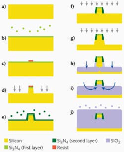
In another development that could be key to practical integrated photonics, Nicolás Sherwood-Droz and two other researchers from Cornell University (Ithaca, NY) have created an approach to fabricating integrated photonics that replaces the conventional intricate silicon-on-insulator approach with an entirely CMOS-compatible bulk-silicon method using common masking and oxidation techniques. The process can be put into practice on a standard CMOS fabrication line. In the technique, silicon waveguide are created by oxidation that pinches off the silicon under the waveguide (see Fig. 5). "It's simply a matter of time before computer architects find themselves with power and bandwidth requirements that electronics cannot match, and which photonics will provide, and then we'll see many more electronics companies begin to integrate these types of processes in their fab lines," says Droz.Full-color (red-green-blue) laser picoprojectors are the dream of cell-phone manufacturers but will be practical only when cost comes down—for example, by replacing today's frequency-doubled green lasers with direct green diode lasers. Microvision (Redmond, WA) announced that it has integrated the first green diode-laser samples from two leading manufacturers into picoprojector benchtop prototypes. While the company wouldn't say who made its green diode lasers, it noted that based on public information there are five direct-green players: Osram, Kaai (now Soraa), Nichia, Rohm, and Sumitomo. "All of them have different specifics, but we have seen 510 to 520 nm and output power of 50 mW," says Sid Madhavan of Microvision.
Another company with an all-diode-laser full-color picoprojector module prototype is Explay (Tokyo, Japan); the company says that the module has a resolution of 852 × 480 pixels and a brightness of 14 lm, and can project an image to a distance of 20 to 200 cm. The module has a volume of 7 cm3 and is 7 mm thick.
Soraa (Fremont, CA) continues to make rapid progress in its development of direct green and blue diode lasers for commercialization, says Paul Rudy, the company's vice president of business development. "In the green regime, we have demonstrated 520 to 525 nm singlemode lasers with about 2% wall-plug efficiency (WPE) and more than 60 mW of output power continuous wave. In the blue regime, we have demonstrated singlemode lasers with over 23% WPE, 750 mW of output power, and projected lifetimes in the 10,000 h range. Green laser lifetime testing is underway with promising initial results."
In a fundamental advance, scientists at the University of Tübingen (Tübingen, Germany) have implanted a light-sensitive, externally powered microphotodiode array behind the retinas of blind human patients (see Fig. 6).6 The array receives light through the patient's eye lens and stimulates retinal cells, generating an image with a 38 × 40 pixel resolution, which has allowed three previously blind people to locate objects on a table. One patient, blind for several years, could name objects like knives, forks, and different types of fruit, and could read complete words made of large letters.Not your average photonics
And finally, a brief mention of some photonic devices (either real, or as-yet theoretical) that illustrate some of the more peculiar phenomena that are or could be part of the physics of light.
An electromagnetic "black hole" was experimentally realized by researchers at Southeast University (Nanjing, China). The device actually has no gravitational effects and is a 2D metamaterial that serves as an omnidirectional optical absorber in the microwave region. But the radially varying permittivity does simulate the gravitational pull a real black hole exerts on photons, pulling all light within it. Microwaves with an 18 GHz frequency and any polarization get sucked into the device and absorbed.
In a photonic setup that is not a simulation or imitation, but exhibits a fundamental effect of gravitational black holes, researchers from Universitá degli Studi di Milano, INFN sezione di Milano, Universitá dell'Insubria, and Universitá di Milano-Bicocca in Italy, and Heriot-Watt University in Edinburgh, Scotland use a laser pulse filament to create a traveling refractive-index perturbation within fused silica—with the result that actual Hawking radiation, which is normally only produced at the event horizon of a gravitational black hole, is instead created on an optical table. Hawking radiation is a purely quantum effect in which photon pairs arise from nothing, with one pulled into the black hole and the other radiated out into space. In the lab, the traveling index perturbation is what separates the quantum-vacuum-produced photon pairs.
Odder still is the idea that an ordinary photon can change into something called a hidden photon, which can't be absorbed by matter, and then change back into a regular photon. The result would be that the photon could travel through an opaque wall (or the Earth, for that matter). The idea results from some predictions that arise from string theory. To find out if such a thing could happen, a bright source is needed for experimentation. Davide Cadamuro and Javier Redondo of the Max Planck-Institute für Physik (Munich, Germany) propose the Sun as a source, particularly because the transition from ordinary to hidden photon could happen in the Sun's interior.7 One experiment, called the Solar Hidden Photon Search, will essentially consist of sensitive photon detectors in a dark room. Other possible sources of data are existing helioscopes. Quantum weirdness arises again in a proposal by scientists at Louisiana State University (Baton Rouge, LA) in which a polarization interferometer cycles a photon repeatedly within itself—with the important caveat that the absorption loss and the single-pass polarization-rotation angle must be set just right. If all is proper, than the device becomes a quantum tripwire, which can detect intruding objects crossing the light path without the object intercepting or classically influencing the photon. Detection does not reach 100% certainty, but still can be high. The device has not yet been built.
REFERENCES
1. T. Ergin et al., Sciencexpress.org, 10.1126/science.1186351 (Mar. 18, 2010).
2. W. Bai et al., Opt. Exp., 18, 104 (Nov. 8, 2010).
3. M.K. Bhuyan et al., Appl. Phys. Lett., 97, 081102 (2010).
4. A. Mukherjee et al., Appl. Opt., 49, 11 (April 10, 2010).
5. K.K. Chen et al., Opt. Exp., 18, 6 (Mar. 15, 2010).
6. E. Zrenner et al., Proc. Royal Society B, published online before print Nov. 3, 2010, doi: 10.1098/rspb.2010.1747.
7. D. Cadamuro and J. Redondo, arXiv: 1010.4689v1 [hep-ph] (Oct. 22, 2010).
About the Author
John Wallace
Senior Technical Editor (1998-2022)
John Wallace was with Laser Focus World for nearly 25 years, retiring in late June 2022. He obtained a bachelor's degree in mechanical engineering and physics at Rutgers University and a master's in optical engineering at the University of Rochester. Before becoming an editor, John worked as an engineer at RCA, Exxon, Eastman Kodak, and GCA Corporation.
