Photonic Frontiers: Antimonide lasers fill hole in the mid-infrared spectrum

Antimonide lasers may seem the poor relation of the III-V semiconductor diode-laser family. With smaller bandgaps than nitrides, phosphides, or arsenides, antimonides occupy the unfashionable part of the infrared spectrum beyond the 1650 nm end of the fiber-optic communications band. However, fashion is changing, and growing interest in compact room-temperature semiconductor lasers emitting in the mid-infrared (IR) have put antimonide lasers in the spotlight.
III-V antimonide lasers emitting at 1940 nm already are welding transparent plastics, and developers are considering other applications for antimonide diode lasers ranging from molecular sensing to IR countermeasures. They fill a troublesome gap in the diode-laser spectrum between the 1.7-µm-long end of the indium phosphide spectrum and the short-wavelength end of the quantum-cascade laser range at about 4.2 µm. In this range, says Gregory Belenky of the State University of New York at Stony Brook (Stony Brook, NY), "antimonides are the only materials that can provide desirable light sources."
Basics of antimonides
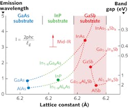
Gallium antimonide, the usual substrate for antimonide lasers, has a lattice constant of 0.61 nm, larger than the analogous gallium arsenide (GaAs) and indium phosphide (InP), and its bandgap energy is 0.726 eV, corresponding to a wavelength of 1.7 µm (see Fig. 1). Two other III-V binary compounds have similar lattice constants, aluminum antimonide (AlSb) at 0.614 nm and indium arsenide (InAs) at 0.606 nm, and in practice all three are called "antimonides" because they are similar to GaSb (gallium antimonide), despite the fact that InAs doesn't contain any antimony. Binary, ternary, quaternary, and quintary compounds are used that contain Al, Ga, In, As, Sb, and P.
Gallium antimonide got off to an early start as a light emitter when Rubin Braunstein of RCA Laboratories (Princeton, NJ) used it in one of the three initial types of III-V light-emitting diodes he made in 1955; the others were GaAs and InP.1 However, GaSb lagged behind because early developers focused on the shorter wavelengths. Russian researchers first reported room-temperature lasing from double heterostructure AlGaAsSb/GaSb lasers in 1976, and by 1981 had demonstrated laser operation between 1.55 and 1.8 µm, with lowest threshold current of 1.5 to 2.5 kA/cm2 at 1.7 to 1.8 µm.2 However, it soon became clear that InP-based lasers were better for the low-loss window of optical fibers, and the fiber-optic stampede bypassed antimonide lasers.
A few developers continued with antimonide lasers, but they needed innovations to reach longer infrared wavelengths. Double-heterostructure lasers sufficed to reach CW room-temperature operation at 2.2 µm in the early 1990s, and switching to conventional quantum-well lasers boosted performance.3 However, formidable technical obstacles loomed at longer wavelengths. As the bandgap of a semiconductor decreases, Auger decay can drain away an increasing fraction of the excitation energy before it can be channeled into photon emission. Free-carrier absorption losses also increase with wavelength.
Commercial and research lasers
Diode lasers at the short end of the GaSb spectrum are offered commercially. M2K-Laser (Freiburg, Germany) now makes them at wavelengths from 1.87 to 2.2 µm. Output power can reach 1 W from a single laser and 10 W in a 1 cm bar. Dilas (Mainz-Hechtsheim, Germany) uses GaSb in laser welders that weld transparent plastics by focusing 1940 nm light that's absorbed strongly by C-H bonds in the polymer.Meanwhile, developers have steadily increased power and pushed room-temperature emission to longer wavelengths (see Fig. 2). The plots of output power as a function of drive current for lasers represent a decade of progress by Belenky's group at the State University of New York in Stony Brook. All were quantum-well antimonide lasers with electrons and holes confined in the same layer, called Type 1 lasers. In 1999, they had not yet produced CW room-temperature output at 2.7 µm. By 2004, they had reached that goal and were trying to make 2.9 µm antimonide lasers emit CW at room temperature. Now the group is pushing for CW operation of 3.5 µm diodes at room temperature. Belenky says he's not there yet, but that he sees no fundamental limitation that could stop him.
Continuous-wave power at room temperature has also risen steadily, now exceeding one watt at wavelengths between 2 and 2.5 µm. Minimum threshold currents for lasers emitting in that band are around 100 A/cm2, comparable with the best reported in GaAs, Belenky says. At CLEO last year, Markus-Christian Amann's group at the Technical University of Munich (Garching, Germany) measured threshold currents as low as 74 A/cm2 in a CW room-temperature laser emitting at 2.65 µm, with a Ga0.57In0.43As0.14Sb0.86 quantum well sandwiched between GaSb barriers.4
Further refinements are needed for longer-wavelength lasers. Belenky's group reports compressive strain, improved carrier confinement, and additional quantum wells can reduce Auger processes, allowing room-temperature laser operation beyond 3 µm. In 2008, the group produced CW lasing at wavelengths as long as 3.36 µm at 12°C.5 A barrier layer of the quintary compound AlInGaAsSb improved confinement in the InGaAsSb quantum wells in those devices, and similar structures allowed the same group to generate up to 300 mW at 3 µm and up to 65 mW at 3.32 µm, also close to room temperature.6
Interband cascade lasers
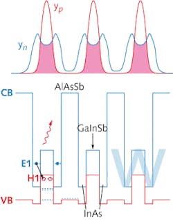
The leading approach deeper in the mid-infrared is the interband cascade laser, which Jerry Meyer of the Naval Research Laboratory (Washington, DC) calls "a hybrid between a normal diode laser and a quantum-cascade laser." The diode part of the hybrid is a Type 2 junction, with the conduction band minimum in an InAs layer and the valence band maximum in an adjacent GaInSb layer. Electrons cascade through a series of layers, going from conduction band to valence band in an adjacent GaInSb layer, then back to the conduction band in a second InAs layer (see Fig. 3).Holes also cascade through an interband cascade laser, unlike in quantum-cascade lasers, which carry only electrons. The multiple layers in the interband cascade laser offset the low gain of the Type 2 structure, but require a higher operating voltage than an individual diode. Interband cascade lasers typically have several stages, compared to 30 or 40 for quantum-cascade lasers, and emit higher-energy photons.
Interband cascade lasers are not as mature as conventional diodes, and can't match their operating powers, but they work best at the long end of the mid-IR band, while conventional diodes work best at shorter wavelengths. The two types essentially operate in different ends of the mid-IR band. Thus the two are more complementary than competitive.
For a while, the highest CW operating temperature for an interband cascade laser, 288 K, was for a 10-stage device emitting at 4.1 µm.7 By refining their devices and reducing the number of stages, to five, Meyer's group then demonstrated CW operation at 3.75 µm at temperatures to 319 K, the first interband cascade laser to exceed room temperature. Output at 300 K reached 10 mW.8 Since then they have pushed to higher temperatures and powers. A laser with a 4.4-µm-wide ridge recently emitted CW at 3.7 µm at temperature to 335 K, and one with a 10 µm ridge and coated facets emitted up to 59 mW CW at 298 K, Meyer says.9
Outlook
Other groups also are working on antimonide lasers. At last year's CLEO, a team from the National Research Council of Canada (Ottawa, Ontario) described single-mode distributed-feedback antimonide lasers emitting 11 mW CW at 2.4 µm when operated at 293 K. Designed for gas sensing, they could be tuned by varying the drive current.10 A team from the University of Montpellier 2 (Montpellier, France) reported room-temperature CW operation at 2.2 µm of an antimonide laser deposited on a GaAs substrate, despite the substantial lattice mismatch, which could lead to growing antimonide lasers on easier-to-obtain GaAs substrates.11
The advance of antimonide lasers promises to plug a maddening gap in the mid-IR laser spectrum, providing new laser sources for applications from medical diagnostics and measurements of molecular gases to infrared countermeasures. So far commercial versions are only available at wavelengths to 2.2 µm, but research labs are making steady progress on practical lasers emitting longer wavelengths to close the gap.
FURTHER READING
L. J. Olafsen et al., "Antimonide Mid-IR Lasers," pp. 69-143 in Hong K. Choi, ed., Long-Wavelength Infrared Semiconductor Lasers, (Wiley, Hoboken, NJ, 2004).
ACKNOWLEDGMENT
Gregory Belenky wishes to acknowledge AFOSR (Air Force Office of Scientific Research, Washington, D.C.) and ARO (Army Research Office, NC) for its continued support.
REFERENCES
1. R. Braunstein, Phys. Rev. 99, p. 1892 (Sept. 15, 1955).
2. L. M. Dolginov et al., IEEE J. Quant. Electronics 17, p. 593 (May 1981).
3. H. K. Choi and S. J. Eglash, Appl. Phys. Lett. 59, p. 1165 (1991).
4. K. Kashani-Shirazi et al., CLEO 2009, paper CtuGG5.
5. L. Shterengas et al., Appl. Phys. Lett. 93, 011103 (2008).
6. L. Shterengas et al., Electron. Lett. 45, p. 942 (2009) and G. Belenky et al., Semicond. Sci. Technol. 24, p. 115013 (2009). doi:10.1088/0268-1242/24/11/115013
7. C. L. Canedy et al., J. Vac. Sci. Technol. B 26, pp. 1160-1162 (May 2008).
8. M. Kim et al., Appl. Phys. Lett. 92, p. 191110 (2008).
9. I. Vurgaftman et al., New J. Phys. (in press)
10. P. J. Barrios, CLEO 2009, paper CTuGG3 and Appl. Phys. Lett. 95, p. 041104 (2009); doi:10.1063/1.3189814.
11. L. Cerutti et al., CLEO 2009, paper CtuGG4.
About the Author
Jeff Hecht
Contributing Editor
Jeff Hecht is a regular contributing editor to Laser Focus World and has been covering the laser industry for 35 years. A prolific book author, Jeff's published works include “Understanding Fiber Optics,” “Understanding Lasers,” “The Laser Guidebook,” and “Beam Weapons: The Next Arms Race.” He also has written books on the histories of lasers and fiber optics, including “City of Light: The Story of Fiber Optics,” and “Beam: The Race to Make the Laser.” Find out more at jeffhecht.com.


