Thin-film thermoelectric technology makes optoelectronics 'cool'
PAUL A. MAGILL
Embedded thermoelectric coolers (eTECs) are smaller and thinner than conventional products and show promise for direct integration in laser diodes and other optoelectronic devices using industry-standard manufacturing methods. Thin-film eTECs and TECs have demonstrated a heat-pumping capacity that far exceeds that provided by traditional bulk TEC products, which makes eTECs ideally suited for high-heat-density applications. In addition to the increased heat-pumping capability, the use of thin films will allow for truly novel implementations of thermoelectric devices, particularly for cooling and temperature control of optoelectronic components.
Optoelectronic devices have traditionally used thermoelectric coolers (TECs) for precision temperature control to maintain wavelength integrity and improve diode output levels. A major trend for photonics in telecommunications has been the move to more integrated packaging that is smaller and simpler to enable a lower-cost structure. This in turn is opening the door for higher-volume manufacturing. In the course of this transition, however, conventional TEC solutions have become increasingly difficult to utilize, as conventional bulk thermoelectric technology has not kept pace with the size and power density requirements for next-generation devices.
In addition to the issue of smaller packaging and higher heat densities, eTECs address junction temperature of light-emitting diodes (LEDs), which can directly affect the performance and longevity for some devices. As the junction temperature rises, a significant loss of output (luminosity) can be expected. The forward voltage of an LED is also dependent on the junction temperature and as the temperature rises, the forward voltage decreases, which can cause excessive current drain on other LEDs in the array. This in turn would lead to thermal runaway conditions and ultimately to the failure of the device. High temperatures can also affect the wavelength of an LED fabricated using gallium arsenide, gallium nitride, or silicon carbide.
Core technology
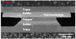
The core technology for some thin-film thermoelectric coolers is the thermal copper-pillar bump. The "thermal bump" is a thermoelectric structure made from a thin-film thermally active material that is embedded into flip-chip interconnects (in particular copper-pillar solder bumps) for use in electronics packaging (see Fig. 1).
The thermal bump was developed as a method of integrating active thermal management functionality at the chip level in the same manner that transistors, resistors, and capacitors are integrated in conventional circuit designs today. Unlike conventional solder bumps that provide an electrical path and a mechanical connection to the package, thermal bumps act as solid-state heat pumps and add thermal management functionality locally on the surface of a semiconductor chip or other electrical component.
Thermal bumps today are already extremely small: 238 µm in diameter by 60 µm high, with the capability for scaling to different sizes. The size of the thermal bump enables the integration of thermal management capabilities at the wafer, die, or package levels (see Fig. 2).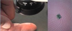
The thermal bump makes use of the thermoelectric effect, which is the direct conversion of temperature differences to an electrical voltage and vice versa. Simply put, a thermoelectric device creates a current flow when there is a temperature difference on each side of the device, or alternatively when a voltage is applied to it, a temperature difference is created. This effect can be used to generate electricity, to measure temperatures, to cool objects, or to heat them.
For each bump, thermoelectric cooling occurs when a DC current is passed through the bump. The thermal bump pulls heat from one side of the device and transfers it to the other as current is passed through the material. This is known as the Peltier effect. The direction of heating and cooling is determined by the direction of current flow and the sign of the majority electrical carrier in the thermoelectric material. When combined with a feedback mechanism, the temperature of a target surface can be controlled and maintained by systematically toggling the direction of the current flow.
The use of thin films in thermoelectric solutions offers many advantages in terms of size, efficiency, and power-pumping capability. Thin-film modules add as little as 100 µm of thickness to a heat spreader, enabling unobtrusive integration close to the heat source. eTECs can pump heat densities of 150 W/cm2 or greater. While bulk TECs pump approximately 10 to 15 W/cm2 on average, eTEC modules pump 10 to 20 times that capacity. This makes thin-film eTECs ideally suited for applications involving high heat-flux flows.
Discrete modules
Thermoelectric cooling and temperature control of laser diodes and high-heat-flux devices such as semiconductor optical amplifiers (SOAs) can now be accomplished using discrete modules. The eTEC OptoCooler UPF4 is an example of a discrete module that can cool and control temperature of laser diodes. The module was developed in response to market demand for microscale cooling solutions that improve the performance of electronics without sacrificing efficiency. With four thermal bumps at its core, the OptoCooler module contains two p-n couples sandwiched between top and bottom headers of aluminum nitride (AlN). This design enables the OptoCooler module to be embedded directly into an optoelectronic package to deliver more than 45°C of cooling and remove a maximum of 420 mW of heat at an ambient temperature of 25°C in an active footprint of only 0.55 mm2 (see Fig. 3).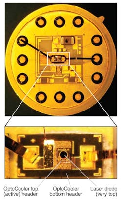
As a discrete module embedded in a laser-diode package, the OptoCooler can pump a heat density up to 78 W/cm2 at 25°C—an industry first—with a total heat-pumping capability of 0.4 W at 25°C. This approach is ideal for maintaining the diode's optimal operating conditions and performance.
Slightly larger thermoelectric modules are ideally suited for the cooling and temperature control of optoelectronic devices such as SOAs, enabling the integration of thermal management capabilities directly into a package. For example, the OptoCooler UPF40 module can pump a heat density of up to 72 W/cm2 at 25°C, and as a result, it can move a maximum of 3.7 W of heat with an active footprint of 5.1 mm2.
Discrete cooling modules are capable of operating with heat fluxes exceeding five times that of conventional thermoelectric coolers. In addition, modules with extremely small footprints open up new thermal management capabilities in electronics that were previously unavailable.
Making connections
The electrical power source of the eTEC module in various packages may be directly connected to the chip circuitry. Such direct connections enable on-board temperature sensors and driver circuitry to control discrete modules, such as the OptoCooler modules, in a closed loop fashion to maintain optimal performance.
The device pumps heat and creates heat in the course of pumping, both of which must be rejected into the substrate or board. Provision of a highly conductive thermal pathway for the superfluous heat is beneficial to the performance of the module. For TO-56 packages, this is typically accomplished through the electrical connections themselves, and depending on the operating characteristics, this level of thermal management might be sufficient. For packages with higher heat densities, mechanical systems using thermal clamps or heat sinks would be necessary to remove heat from the overall package.
The smaller, thinner form factor of eTECs enables a new approach to electronic thermal management that focuses on providing appropriate cooling when and where it is needed in the optoelectronic system. This solution involves the integration of thin-film thermoelectric material into the solder bumps that are used for electronic interconnects and/or the embedding of thin-film modules into the package. Active thermal management at the surface of the device is a fundamentally new methodology for achieving temperature uniformity and control in optoelectronic devices.
PAUL A. MAGILL is vice president of marketing and business development at Nextreme Thermal Solutions, 3908 Patriot Dr., Suite 140, Durham, NC 27703-8031; e-mail: [email protected]; www.nextreme.com.