Many people would agree that art and science inhabit separate worlds. Few scientists create memorable art, while few artists contribute directly to science. But there is one area in which these two dissimilar worlds touch, and that is commerce. Science begets high technology, which then evolves into mass-manufacturable and profitable consumer goods. Creators of fine art set out to sway people by presenting powerful images—but so do commercial artists, who are the creative power behind iconic images that help sell the same mass-marketed goods. Catching the consumer's eye is key.
Most of the past year's technical achievements in optoelectronics rest solidly in the science and high-technology camp. Advances in lasers, optics, fiberoptics, and light detection have been many in 2001; some favorites of the Laser Focus World editorial staff include better ultraviolet lasers, extreme optics, and exotic-polymer optical fibers. All show great promise at levels ranging from basic research to commercial application.
But sometimes an advance in optoelectronics moves beyond the concrete world of technological research, development, and application into the more nebulous domain of marketing, advertising, and the intent to influence people. The flexible display is one such device. Its future rests not only with the expertise of applications engineers, but also with the ability of marketers and commercial artists to use this product in creative, eye-catching ways. For some technical types, the idea that the success of their laboriously developed device can hinge on a few bright ideas in an advertiser's head may be unsettling. For others, though, the potential of success in the larger consumer market—driven by images, whim, and emotion as much as by technological innovation—may serve as an impetus to think beyond the usual constraints.
Solid-state lasers diversify
As is well-known, Nichia Corp. (Kaminaka, Japan) is the inventor and sole commercial supplier of blue-emitting laser diodes. Efforts at corporate laboratories such as those at Cree (Durham, NC) and Xerox (Palo Alto, CA), as well as work at universities around the world, are resulting in gallium nitride (GaN)-based lasers that may ultimately compete with Nichia's, but for now fall short in lifetime. Research on silicon carbide (SiC) substrates (the Cree approach) for GaN-based lasers is under way at the NASA Glenn Research Center (Cleveland, OH); the effort has resulted in fabrication of SiC free of deleterious atomic-layer steps on its surface (see Laser Focus World, June 2001, p. 34).
There are other ways to make commercially viable small, blue-emitting semiconductor-based lasers. Coherent Inc. (Santa Clara, CA) has sallied forth this year with a compact blue laser based on an optically pumped, frequency-doubled vertical-cavity surface-emitting laser. The first publicly introduced version emits at 488 nm and is designed to replace similarly emitting argon-ion lasers that are many times larger and eat up fifty times more electrical power; the laser will be used in analytical instrumentation and semiconductor wafer inspection.
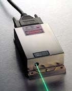
At the heart of the Coherent device are quantum-well structures that provide gain at 976 nm. An intracavity frequency-doubling crystal converts the emission to the desired 488-nm wavelength. The laser produces 20 mW of optical output with a TEM00 beam profile and has an optical noise less than 0.25% root mean square. Coherent has also introduced a similar laser emitting at 460 nm, also competing with the argon-ion laser and intended for digital imaging systems, inspection systems, and bioinstrumentation (see Fig. 1).Larger diode-pumped solid-state (DPSS) ultraviolet (UV) lasers based on traditional nonsemiconductor gain media are also making their mark. An example is the 500-mW frequency-quadrupled continuous-wave Nd:YVO4 laser introduced this year by Spectra-Physics (Mountain View, CA). The wavelength is produced by frequency doubling a 532-nm doubled DPSS laser with an external resonator in a double-delta geometry. The resonator contains two piezo-translated prisms, one providing geometry-invariant cavity-length stabilization for fast response to acoustic noise, and the other used to match the build-up cavity length to the resonator length. The design is simple and stable.
Another of this year's DPSS UV solid-state lasers by Spectra-Physics emits 4.5 W of 355-nm light with a TEM00 (M2 less than 1.2) output. Also based on a vanadate laser, this version is modelocked via a saturable Bragg reflector, producing 10-ps pulses at a repetition rate of 80 MHz.
Aiming for maximum output, researchers at Eanuc Ltd. Laser Research Laboratory (Minamitsuru-Gun, Japan) have constructed a diode-pumped slab Nd:YAG that emits 6.6 kW, and in another configuration achieves an electrical-to-optical efficiency of 16% at 4.0 kW (see Laser Focus World, July 2001, p. 30). The 6.6-kW output is the result of superposition of two orthogonally polarized beams. A 3.0-kW version in pulsed operation reached an optical-to-optical efficiency of 49%. Another group at Mitsubishi Electric Corp. (Amagasaki, Japan) designed and built a 320-W DPSS laser with a wallplug efficiency of 28% and a beam quality (M2) of 4.
Quantum-cascade (QC) lasers are increasing in wavelength range and usefulness. Far-infrared versions emitting at wavelengths as long as 24 µm find use in trace-gas sensing: for example, the monitoring of atmospheric methane and nitrous oxide (see Laser Focus World, September 2001, p. 65). Researchers at Lucent Technologies (Murray Hill, NJ) and Applied Optoelectronics Inc. (Sugar Land, TX) have developed a QC laser that emits two wavelengths simultaneously by tapping into the cascade at two different points (see Laser Focus World, September 2001, p. 65). Such a laser could conceivably be used for sensing two gases at once.
LEDs will light your home—someday
The days of light-emitting diodes (LEDs) as faint red and green indicator lights and nothing more are long gone. With the advent of high-brightness aluminum indium gallium phosphide red-emitting LEDs and aluminum indium gallium nitride blue- and green-emitting LEDs, the devices will soon be serious contenders for at least some niche lighting applications (see Laser Focus World, September 2001, p. 81). As in other optoelectronic technologies that have crossed over from the laboratory widget stage into the consumer world, LEDs for lighting have become the object of big-money funding by the likes of Uniroyal Technology Corp. (Sarasota, FL), LumiLeds (a joint venture between Agilent Technologies of San Jose, CA and Philips Lighting of Somerset, NJ), Cree, and others.
White-light LEDs made by combining red-, green-, and blue-emitting chips may have problems with color uniformity as they age; therefore, devices based on blue-emitting LEDs combined with white-light or yellow (complementary to blue) phosphors have curried favor with those searching for high reliability. Cree has gone one step further than the blue and pushed the emitting wavelength of its high-brightness LEDs to the edge of the UV, permitting more efficient use of phosphors. The 12-mW, 405-nm-emitting LEDs are intended for automotive, mobile-device, and other consumer applications.
Efficient packaging of LEDs is another way to up their effectiveness, especially for home lighting. Engineers at NorLux Corp., a division of Uniroyal, have packaged LED chips in dense hexagonal arrays to make intensely bright, rugged units in both single-color and white-light versions (see Laser Focus World, July 2001, p. 16).
Optics find esoteric and everyday uses
Optics often aid in probing the great and small; two fundamental early examples are Galileo Galilei's telescope, used by him to discover Jupiter's moons, and Antony van Leeuwenhoek's microscopes, which made possible the discovery of single-celled organisms. Though perhaps no future advances in classical optics will be as fundamental as these two, progress continues apace. Researchers at Infineon (Munich, Germany), M. Theiss Hardware and Software, and Aachen University of Technology (both of Aachen, Germany) have created a type of short-pass optical filter, potentially useful for astronomy, that is based on passing light through arrays of micrometer-sized holes in silicon (see Laser Focus World, April 2001, p. 36). Long-wavelength light diffracts and is absorbed by the channel walls, while short-wavelength light passes through.To help probe the world of the small, researchers at the Photonics Center at Boston University (Boston, MA) have developed a hemispherical solid-immersion lens of silicon that, when pressed against the backside of an integrated-circuit (IC)-containing wafer, allows ordinary low-power infrared microscope objectives to image IC features to a demonstrated 0.23-µm (and theoretical 0.14-µm) resolution (see Laser Focus World, September 2001, p. 18). The lens images at a numerical aperture of up to 3.4.
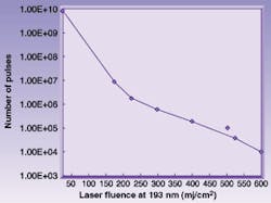
Deep-UV optical coatings find application in laser-assisted in-situ keratomileusis (LASIK) and in lithography. Acton Research Corp. (Acton, MA) has developed 193-nm optical coatings with high damage resistance and durability for use in LASIK eye surgery (see Fig. 2).The high repetition rates and low fluence characteristics of deep-UV lithography lasers can present expected and unexpected damage considerations for optical coatings. At 193 nm and especially 157 nm, the amount of absorption within the coating helps determine the damage resistance and ultimately the lifetime of the coating. A transmission measurement alone cannot determine the amount of absorption within a coating and can lead to early and unpredictable coating failure. For this reason, Acton Research measures both reflectance and transmission of its lithographic optical coatings in vacuum-purged or atmospheric conditions to simulate the actual environment in which the optics will be used, says Michael Case, vice president of R&D.
Researchers at the company also found that continuous high-repetition-rate deep-UV laser exposure can dehydrate coatings over time, causing potential failure when the laser is turned off and the coating is allowed to rehydrate. Careful selection of coating designs, materials, and processes has allowed Acton Research to produce coatings with high resistance to dehydration-induced damage. At 193 nm, coating lifetimes now exceed 7 billion pulses at 20- to 40- mJ/cm2 pulse energies and 400-Hz repetition rate. At 157 nm, lifetimes greater than 200 million pulses are possible and are expected to increase dramatically over the next 12 months as more research is completed, notes Case.
An optical system constructed by physicists at the University of Murcia (Murcia, Spain) probes the human eye (see Laser Focus World, February 2001, p. 32). The system uses a set of optics that produces an array of small images serving both as an imager and Hartmann-Shack wavefront sensor. The point-spread function of the eye is derived, allowing a corrected image to be calculated. Knowing the point-spread function could allow high-quality correction of the eye's aberrations by use of either contact lenses or laser surgery.
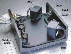
Dynamic control of elements in laser-based optical systems can minimize misalignments resulting from vibration, thermal gradients, and mechanical creep. Fast-steering mirrors (FSMs) developed at Newport Corp. (Irvine, CA) have phase and amplitude bandwidths exceeding 300 Hz; combined with position-sensing detectors and drive electronics, the FSMs keep laser beams pointing in the right direction in applications ranging from semiconductor manufacturing and inspection to telecommunications (see Laser Focus World, October 2001, p. S13). The use of active beam stabilization in laser-based instruments can simplify design, increase reliability, improve performance, and cut manufacturing and repair costs. In one example, two FSMs provide closed-loop tilt compensation (see Fig. 3).Optical diffusers can be fabricated that scatter virtually all light within a specified beam distribution—either uniform or nonuniform—with virtually no backscatter, chromatic dispersion, or transmitted zero-order beam. Engineers at Ledalite Architectural Products (Langley, B.C., Canada) have developed such a diffuser for architectural lighting based on kinoform holograms (see Laser Focus World, September 2001, p. 24). The phase-only surface-relief diffusers were designed using a combination of empirical and theoretical methods and produce a variety of isotropic and anisotropic diffusion patterns at 95% transmission efficiency.
Dense WDM channels, new holey fibers
The capability of a leading-edge fiberoptic communications system based on wavelength-division multiplexing (WDM) is measured both by the maximum possible data rate and the distance between electronic repeaters. The push to increase and test both at the same time results in a mix of claims that are not always directly comparable. One result that stands out is the announcement by Alcatel (Paris, France) of an optical submarine transmission test that reached a 1.6-Tbit/s capacity over a 321-km unrepeatered distance. The results were achieved using cascaded Raman amplification and 160 wavelengths that fell within the C-band at a 25-GHz spacing.In the experiment, Raman pumps were positioned in a cascaded configuration and arranged in the opposite direction of the signal. In addition to two pump sources at the standard wavelength of 100 nm below the signal, another pump at 90 nm below the pump wavelengths was used, allowing a high-power source to boost two low-power sources. The two low-power sources then amplified the transmission signals. This setup is less expensive than current systems that require the use of two high-power pumps.
In a further honing of WDM, Essex (Columbia, MD) is developing hyperfine WDM with channel spacing as close as 50 MHz. Essex announced that four companies would field-test its equipment to transmit 2.5 Gbit/s with channel spacing of 6.25 GHz—a spacing dense enough that 16 channels fit within the 100-GHz bandwidth of a normal single 40-Gbit/s channel.
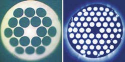
Optical fiber containing arrays of holes that parallel the fiber axis—so-called holey fibers—have properties different from those of conventional fibers (see Laser Focus World, May 2001, p. 207). An array with a central defect can guide light along the defect, either by an effective refractive-index difference or by Bragg reflection. A glass holey fiber with a small-enough central defect has anomalous dispersion that can create white light from monochromatic light via nonlinear interactions with the material. Now, scientists at Redfern Polymer Optics (Sydney, Australia) and the Kwangju Institute of Technology (Kwangju, Korea) have created polymer—rather than glass-based–holey fiber. Plastic provides a greater choice of material properties and places fewer restrictions on the pattern of holes; the pattern also does not partially collapse during fabrication as sometimes happens with glass. The fiber can be made single- or multimode (see Fig. 4).Applications draw on optoelectronics
Optical interferometry takes many forms and has many uses, from distance measurement to wavefront-error characterization to the quantification of mechanical strain. In the last category, a group at the University of Loughborough (Leicestershire, England) has developed a speckle holographic interferometer to test stresses on the human body, including bone (see Laser Focus World, April 2001, p. 95). Dual-beam illumination sensitizes the instrument to motion purely along the axis of illumination, allowing the extraction of a single in-plane axis of motion. Analysis of a human jawbone by the interferometer revealed how the jaw transferred load around the bone without damaging teeth.In cavity ringdown spectroscopy, a short laser pulse makes many round trips through a sample-filled cavity; the decay of the exiting train of pulses provides absorption information. The technique has matured, allowing researchers to measure the spectrum of a form of carbon (C9) at 5 µm, as well as the oxygen-hydrogen stretching bands of methanol, ethanol, and propanol clusters (see Laser Focus World, May 2001, p. 159). The spectrometer uses an alexandrite laser to provide continuous coverage of the mid-infrared.
Adaptive cruise control (ACC) for automobiles, based on lidar with an infrared semiconductor-laser source, is being introduced by automakers (see Laser Focus World, October 2001, p. 32). The speed of an ACC-equipped vehicle increases or decreases based on the speed of the vehicle in front of it; a car moving in front of the vehicle from another lane also causes a speed adjustment. In one form, the ACC hardware can detect 15 different targets and measures only 5 x 10 x 11 cm in size.
A digital moiré system developed by researchers at the University of Texas at Austin measures the yarn spacing in fabrics by comparing a computer-generated grating with an image of the fabric itself.1 The moiré image is demodulated and processed with a phase-shifting technique; the relationship between the pitches of the grating and the moiré fringes provides the yarn spacing. The system is robust, measuring fabrics of many different colors, densities, and degrees of coarseness.
Fast-developing complementary metal-oxide semiconductor (CMOS) technology, containing on-chip processing, is becoming important in the field of high-speed imaging (see Laser Focus World, October 2001, p. 79). With their high readout rate, on-chip multiple sampling, and lack of image bloom, CMOS sensors capture high-quality images at rates up to 60,000 pictures per second.
Early this year, genome researchers at the Human Genome Sequencing Consortium and Celera Genomics (Rockville, MD) each published a substantially complete map of the human genome. Genetic research depends in many ways on instruments that use light (see Laser Focus World, May 2001, p. 137). The DNA microarray allows researchers to test a DNA segment under hundreds or thousands of conditions at once; fluorescence helps to determine which genes within a specimen are being expressed. Other techniques based on DNA-coated glass beads—either free-floating and optically manipulated, or set into the ends of optical fiber bundles—offer potential competition to microarrays.
Displays look to the big picture
The swift metamorphosis of organic light-emitting diodes (OLEDs) from glowing laboratory objects into the basis of functional, rugged microdisplays is the result of worldwide effort. Since scientists at Eastman Kodak (Rochester, NY) developed OLEDs in 1987, more than 80 companies and universities around the world have explored the potential of the technology. For example, eMagin Corp. (Hopewell Junction, NY) is now offering a developer's kit containing the company's 852 x 600-pixel color OLED-on-silicon microdisplay (see "OLED/CMOS combo opens a new world of microdisplay," p. 55). The display switches at submillisecond speeds and is viewable at all forward viewing angles; uses include mobile phones, camcorders, and video headsets.As for the flexible display mentioned earlier, it is made by E Ink (Cambridge, MA). In pixelated form, the company's electrophoretic ink technology can be combined with active-matrix transistors—even in printed form—to create flexible displays that may replace paper for some uses (see Laser Focus World, January 2001, p. 16). In nonpixelated form, electronic ink can be incorporated into advertising signs both large and small, in two different ways.
In one form, individually switched areas of electronic ink are formed into shapes—logos, images, or letters—that are switched on and off in sequence (see Fig. 5). In another, even simpler, form, a single field of black-to-white electronic ink placed behind a color overlay with transparent sections is switched on and off. In the latter case, the sign appears no different from a piece of full-color printed glossy cardboard—at least until the sign is switched.A tour by the Laser Focus World staff of the E Ink facility revealed perhaps a dozen of these small signs scattered throughout the building, some hand-shaped and colored by employees to advertise E Ink company events. As each sign flickered, it unavoidably drew the visitor's eye to it. After a second or two, however, it was the message itself that held the viewer's attention. Placed in a supermarket or department store, such signs would have the same attention-grabbing effect, requiring only the deft touch of a commercial artist to create a new and potent advertising tool.
REFERENCE
- B. Xu et al., Opt. Eng. 40 (8), 1476 (August 2001).
About the Author
John Wallace
Senior Technical Editor (1998-2022)
John Wallace was with Laser Focus World for nearly 25 years, retiring in late June 2022. He obtained a bachelor's degree in mechanical engineering and physics at Rutgers University and a master's in optical engineering at the University of Rochester. Before becoming an editor, John worked as an engineer at RCA, Exxon, Eastman Kodak, and GCA Corporation.
